Electronic product design company, schematic to ship
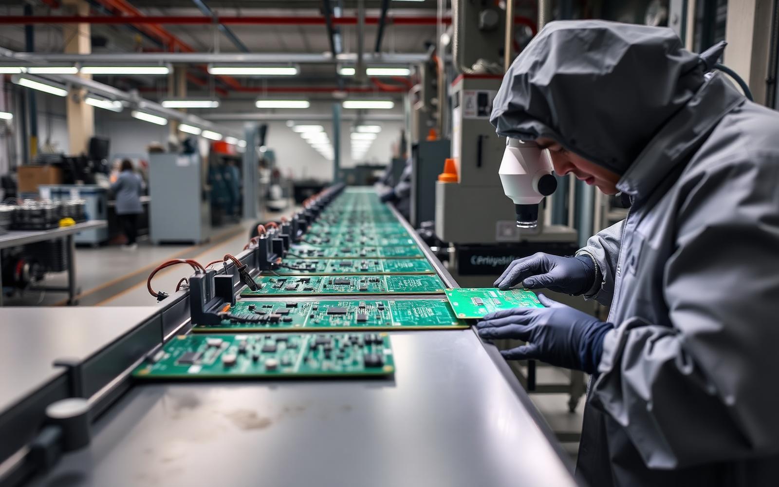
If your product has electronics in it, you need one accountable electronic product design company, not three vendors. LA NPDT runs industrial design, PCB design, mechanical and electrical engineering, firmware, prototyping, and short-run manufacturing in one studio. As an electro
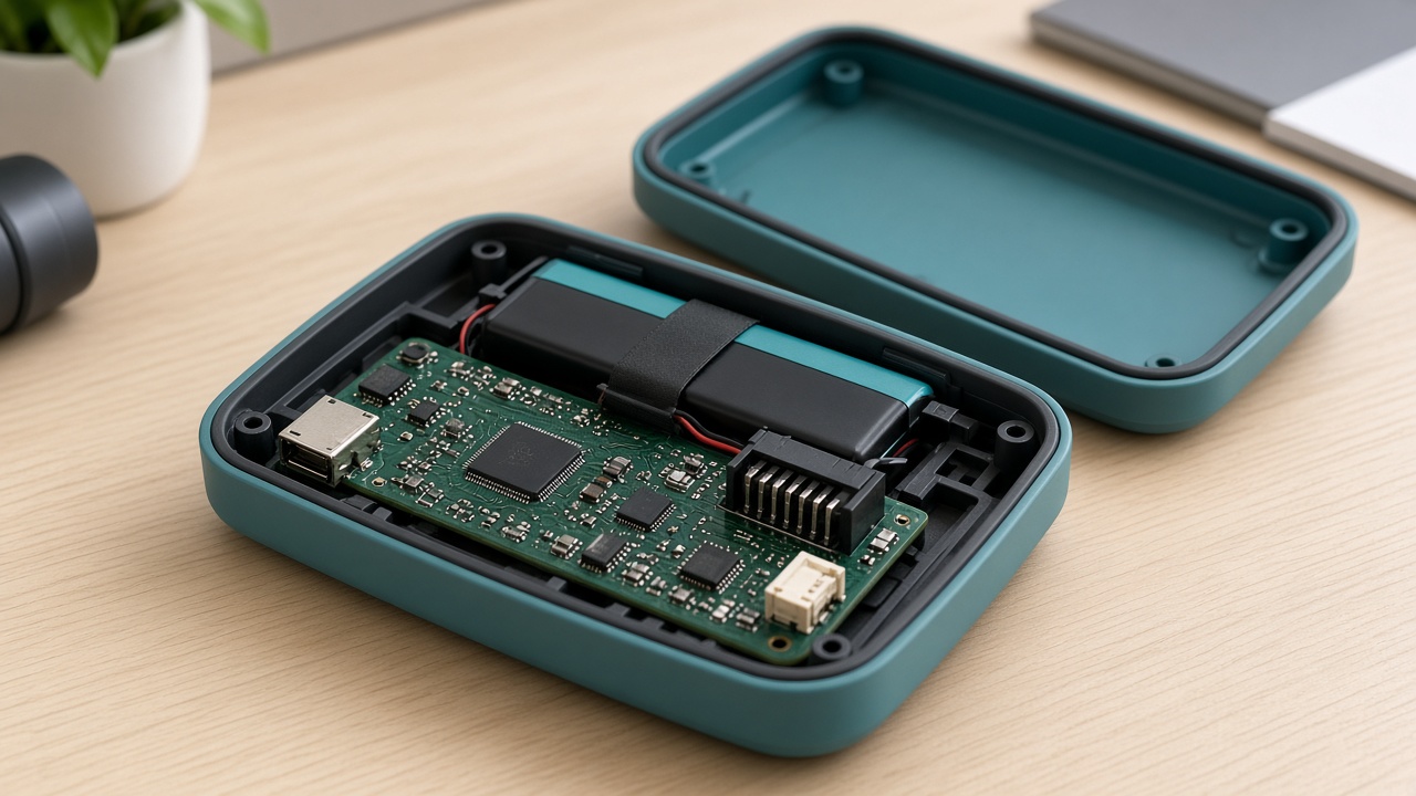
Electronic design services cover schematic capture, PCB layout, firmware and compliance pre-testing for a physical product. LA NPDT designs the board around the enclosure and the battery budget, builds a bring-up prototype, and delivers Gerbers, a bill of materials and test results your contract manufacturer can build from without redrawing anything.
If your product has electronics in it, you need one accountable electronic product design company, not three vendors. LA NPDT runs industrial design, PCB design, mechanical and electrical engineering, firmware, prototyping, and short-run manufacturing in one studio.
As an electronic product design company we ship the board, the enclosure, and the user experience together. No education tax. No coordination tax. No hand-off where your product vision gets watered down.
Electronic design services cover schematic capture, PCB layout, firmware, prototype bring-up and the production handoff for a specific product. A first working board typically takes 8 to 14 weeks and costs $18,000 to $85,000 depending on RF, certification and firmware scope. The table below shows where projects usually land.
| Scope | What it includes | Typical lead time | Typical cost |
|---|---|---|---|
| Simple board | Microcontroller, sensors, power, no radio | 6-9 weeks | $18k-$35k |
| Connected product | BLE or Wi-Fi, app hooks, battery management | 9-14 weeks | $35k-$65k |
| Certified or RF-heavy | Cellular, LoRa, antenna tuning, FCC/CE prep | 14-22 weeks | $65k-$120k |
| Board + enclosure together | Electronics with mechanical and industrial design | 12-20 weeks | $55k-$150k |
Ranges assume one design iteration and a prototype build. Related next steps: prototype design, prototype manufacturing, or estimate your full development cost.
Definition
What does an electronic product design company actually do?
An electronic product design company handles the engineering work behind any product that uses power, signals, or wireless. That includes schematic design, printed circuit board layout, component selection, firmware bring-up, prototyping, and the hand-off to manufacturing. Done right, an electronic product design company treats the electronics, the enclosure, and the user experience as one system. Done wrong, three vendors argue over a deadline.
What it means for you
What it means for you
One team, A to Z, not three vendors and a timezone problem
Most companies stitch together a PCB shop, a mechanical firm, and an offshore assembler. The board lands. The enclosure does not fit. The firmware never met the radio. That is where projects die. Harvard Business Review pegs new-product launch failure rates around 75%. Integration friction between disciplines is one of the biggest reasons.
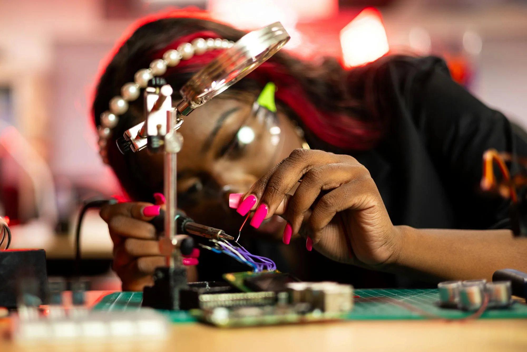
LA NPDT was built so a product with electronics in it can be designed, prototyped, and manufactured by people who sit in the same room. Our electronic design services live next to the same team that handles industrial product design and mechanical CAD. The EE bench sits beside the ID studio, not in another time zone.
- No hassle coordinating several teams
- A dedicated project manager available almost 24/7
- A holistic approach that includes everything beyond the design stage
- A cohesive team ready to take your project from A to Z
Electronic and printed circuit board design
Electronic and printed circuit board design
PCB design that the rest of the product can actually live with
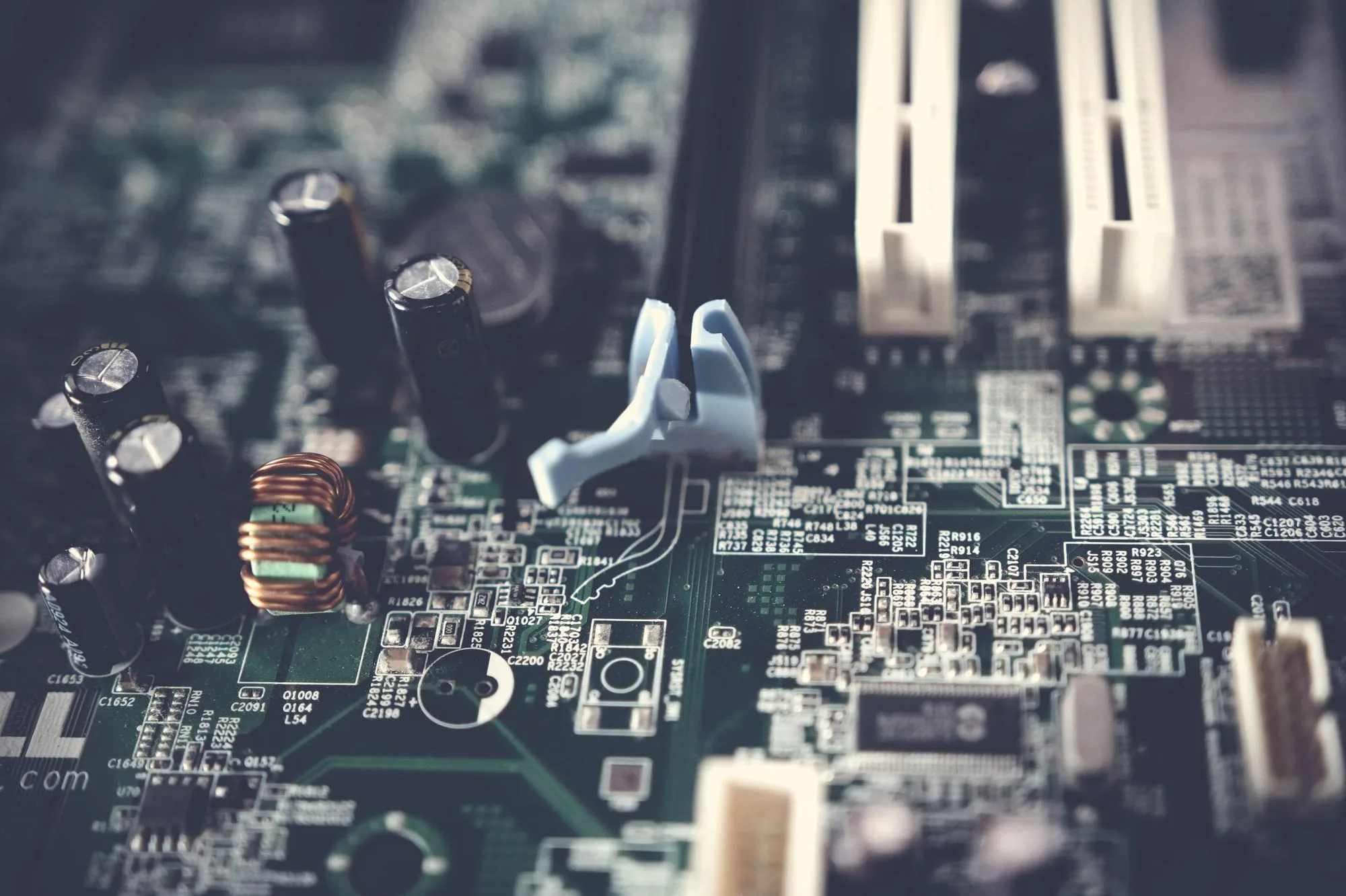
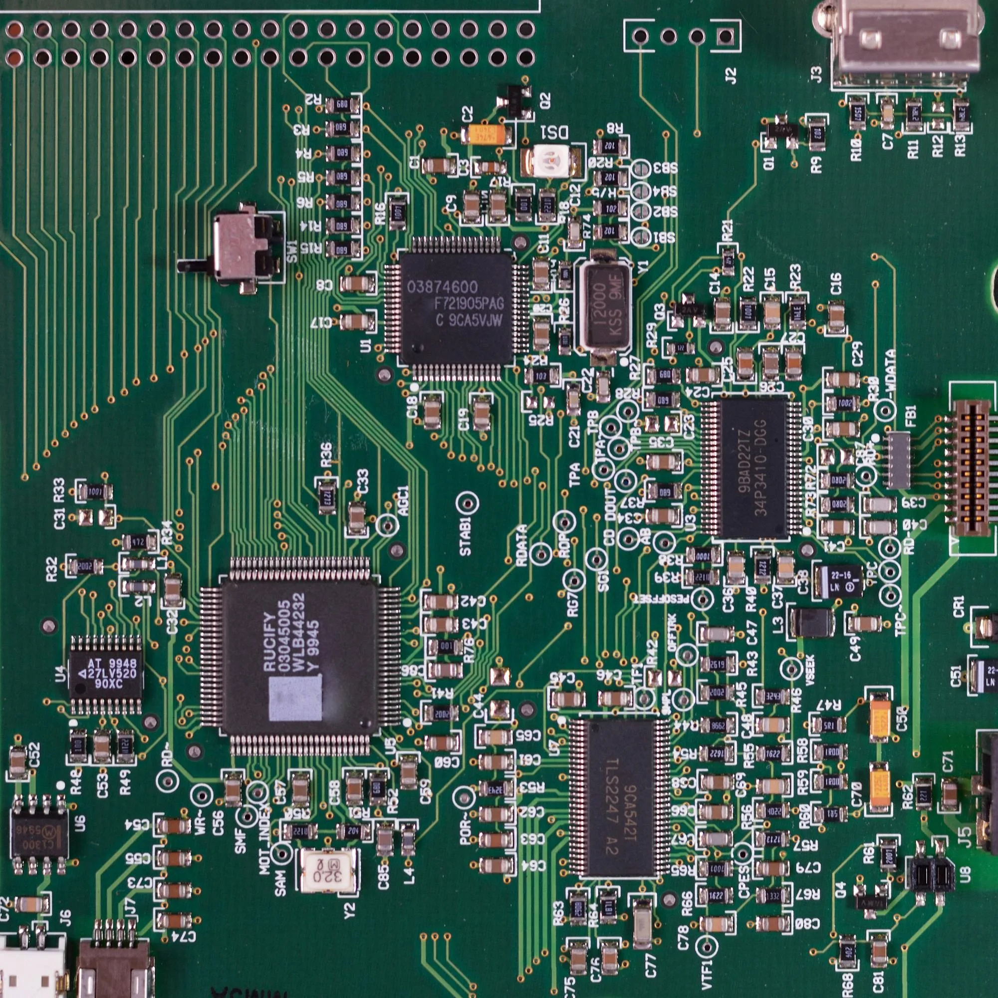
Electronic and printed circuit board design is an integral part of almost every electronic product on the market. It is also one of the most time and resource intensive parts of the process. The choices made on the board determine the product's future: how it scales, how it certifies, and how it gets repaired. FCC equipment authorization rules apply to almost every wireless product sold in the US.
Our designers work meticulously to eliminate potential issues throughout the process. Like everything at LA NPDT, our work as an electronic product design company relies on constant iteration to create custom, turnkey solutions. When the design is locked, it flows straight into in-house rapid prototyping and short-run manufacturing. No layout gets thrown over a wall.
Our process
Our process
Our electronic product design and development process
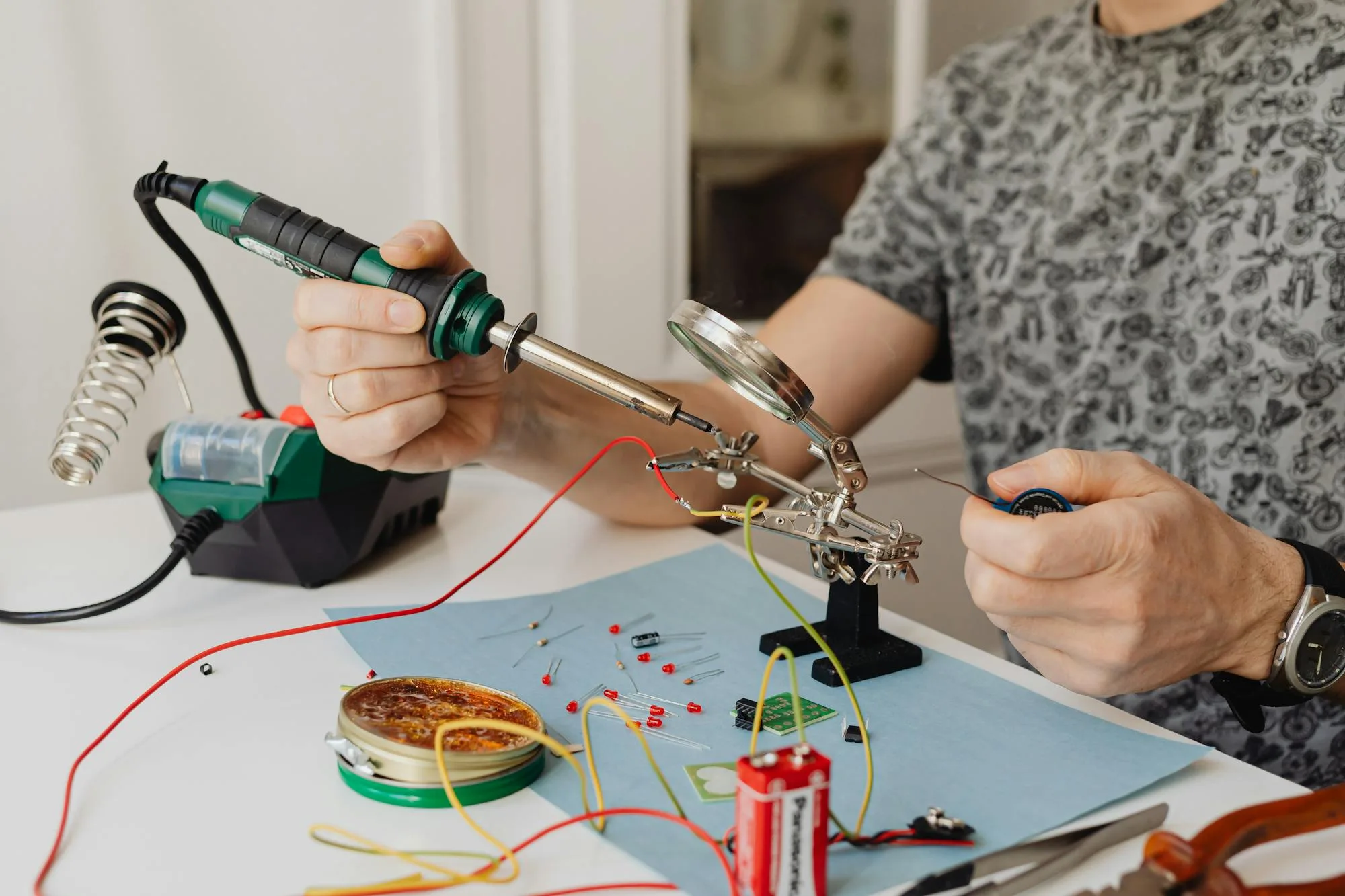
Every program at our electronic product design company begins with an honest read of the problem. We research the existing solutions on the market. Then we decide whether to develop a custom one or use off-the-shelf modules. For first prototypes we lean on off-the-shelf parts on purpose. That saves resources, expedites the launch, and tests product performance and market demand at the lowest possible cost.
After that, we prepare a detailed description of what the product will include. Only then do we start actual PCB development. This is a two-step process: Engineering followed by Prototyping. Each step has its own deliverable and decision point.
Engagement
Engagement
How an electronic product design company runs an electronics program
A repeatable path from concept to a manufacturable electronic product. Hover any phase to expand it. Every phase ends with a deliverable and a go / no-go so you control scope, cost, and timeline.
01 Discovery & requirements Define what the electronics actually need to do. +
We pin down the use case, power budget, environment, certification targets, and the production volume the product is being designed for. Every later trade-off references this brief.
Deliverable: Electronics requirements brief and module strategy.
02 Architecture & component selection Pick the parts before drawing the board. +
We choose the MCU, radios, power tree, sensors, and connectors against a target BOM cost, favoring certified modules where they shorten time to market and custom circuitry only where the product earns it.
Deliverable: Block diagram, candidate BOM, risk list.
03 Schematic design The electrical contract for the product. +
Detailed schematic capture with proper power, signal integrity, and protection considered up front. Reviewed against the requirements brief and the mechanical envelope before any layout begins.
Deliverable: Reviewed schematic package.
04 PCB layout Mechanical reality, not just electrical theory. +
Layout with component placement informed by the enclosure, thermal needs, antenna keep-outs, and assembly economics. Manufacturable trace widths, real stack-ups, and footprints sourced to in-stock parts.
Deliverable: Gerbers, BOM, pick-and-place files.
05 Prototype & bring-up Make it real on the bench. +
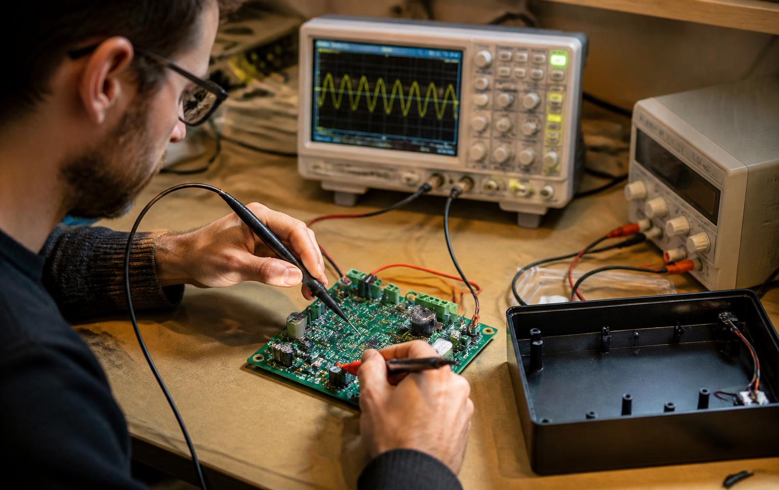
We fabricate and assemble the first prototypes in-house, bring up power and clocks, validate the radios, and write the firmware needed to demonstrate every feature on the requirements brief.
Deliverable: Working prototype, bring-up notes.
06 DFM & short-run Hand off to manufacturing without a fire drill. +
We tighten the design for manufacturability, lock the BOM with second sources, and run a short pilot batch, then transfer to volume production when the pilot says the design is ready.
Deliverable: Released design package and pilot units.
Have an electronic product on the bench?
Tell us what it has to do, where it has to live, and what it has to cost. We will scope an engineering plan that lands a working prototype.
Our electronics design services & PCB design services
Our electronics design services & PCB design services
Designed from the ground up, for your product, not a reference design
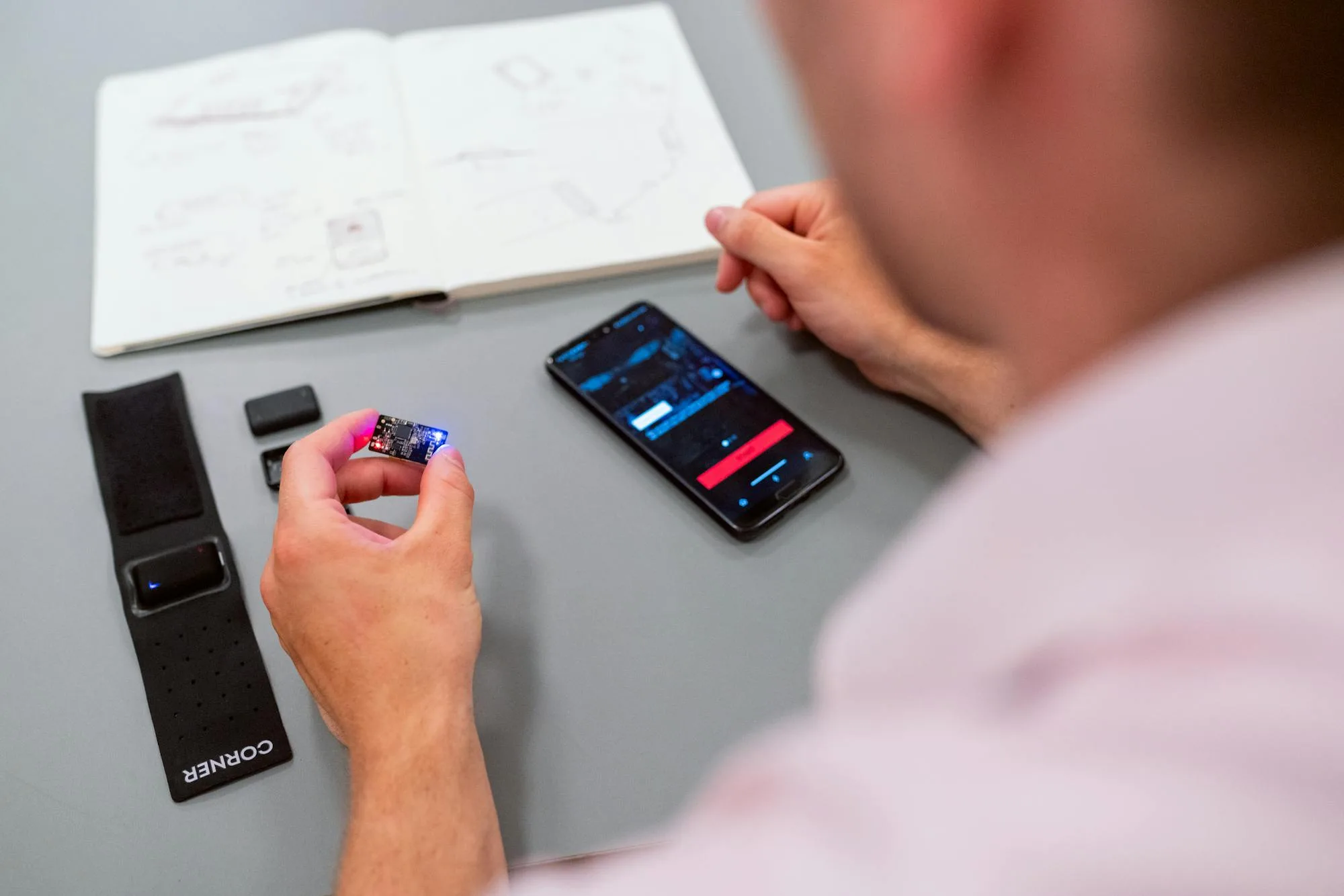
Your new product will likely require a unique printed circuit board design that has never been used or tested. The circuit has to be built from the ground up. As an electronic product design company, LA NPDT does exactly that.
When designing your circuitry and choosing components, our engineers account for several factors:
- What environment will your system live in? Temperature, vibration, moisture, and EMI all change part selection and layout.
- Are there any unique components? Custom sensors, rare connectors, or sole-source parts get flagged early. That keeps the BOM from becoming a sourcing trap.
- What is the production volume and lifetime of your system? A run of 200 and a run of 200,000 are not the same design problem. We scope for the one you are actually building.
These questions shape the choices our experts make. The goal is the most cost-effective electronic system possible. When implementing the PCB into your prototype, we keep it discreet, manageable, and manufacturable. That keeps the product convenient and visually clean for the customer.
Three pillars of the service
Electronic prototype, PCB design & fabrication, short-run production
As an electronic product design company, we own all three. The hand-off between prototype, fabrication, and production is not an email. It is a chair pushed across the studio.
01
Electronic prototype compatibility assurance
Component placement is critical. Your circuit may have electro-mechanical parts or sensors that demand strategic placement. Implementation planning is a crucial part of our electronic design services. We treat it with the utmost importance so the prototype validates the product, not just the schematic.
02
Printed circuit board design & fabrication
When designing your circuitry, components and wires get messy fast. Breadboard prototyping is not sufficient at this point. Our electronic design services keep your circuitry manageable, organized, and manufacturable. Boards are fabricated to spec with real stack-ups and sourced parts.
03
PCB prototype manufacturing & short-run production
Before committing to mass production, you need the design perfected. Testing prototypes is essential. With a PCB prototype you see the electrical system manifested in action. Whether you need a single prototype or a small batch for launch, our PCB design services have you covered.
LA NPDT electronic design services applications
LA NPDT electronic design services applications
Where we have shipped electronic systems
Extensive experience providing electronic design services across analog and digital domains, power, wireless, and embedded systems:
- Digital · Analog · Integrated circuits
- Batteries · Power supply · Audio circuits
- Internet of Things (IoT) · Satellite communication
- Field Programmable Gate Arrays (FPGA)
- NFC · GPS · GSM · Wi-Fi · Wireless · Bluetooth
- Antenna design · Radio Frequency (RF) · RFID
Why it's different
Why it's different
LA NPDT vs a traditional electronics design agency
| Area | Traditional electronics agency | LA NPDT |
|---|---|---|
| Single accountable team | PCB shop, mechanical firm, and CM each own a slice, nobody owns the product | One PM, one schedule, one team owns schematic, enclosure, firmware, and pilot |
| No education tax | You re-explain the product to every new vendor and pay for their learning curve | The team that scoped the product designs the board, so context never resets |
| PCB & enclosure | Designed in isolation, fit issues found late | Co-designed in one studio with the same CAD |
| Schematic and firmware | Two teams, two timezones, one email thread | Same team, same room, same daily standup |
| Component sourcing | Whatever the layout engineer found in stock | Selected against BOM cost with second sources and lifecycle checks |
| Prototype build | Outsourced, weeks of latency per spin | In-house, days per iteration |
| DFM hand-off | Thrown over the wall to a contract manufacturer | Walked into pilot production with the same team |
| Lifecycle support | Each vendor disappears after their deliverable | Same team supports revs, second sources, and re-certification |
| Outcome | A board that works on a bench | A product that ships at cost |
The board, the enclosure, and the firmware are the same project, not three.
LA NPDT electronics philosophy
Pilot & production
Pilot & production
From first article to short-run, under one roof
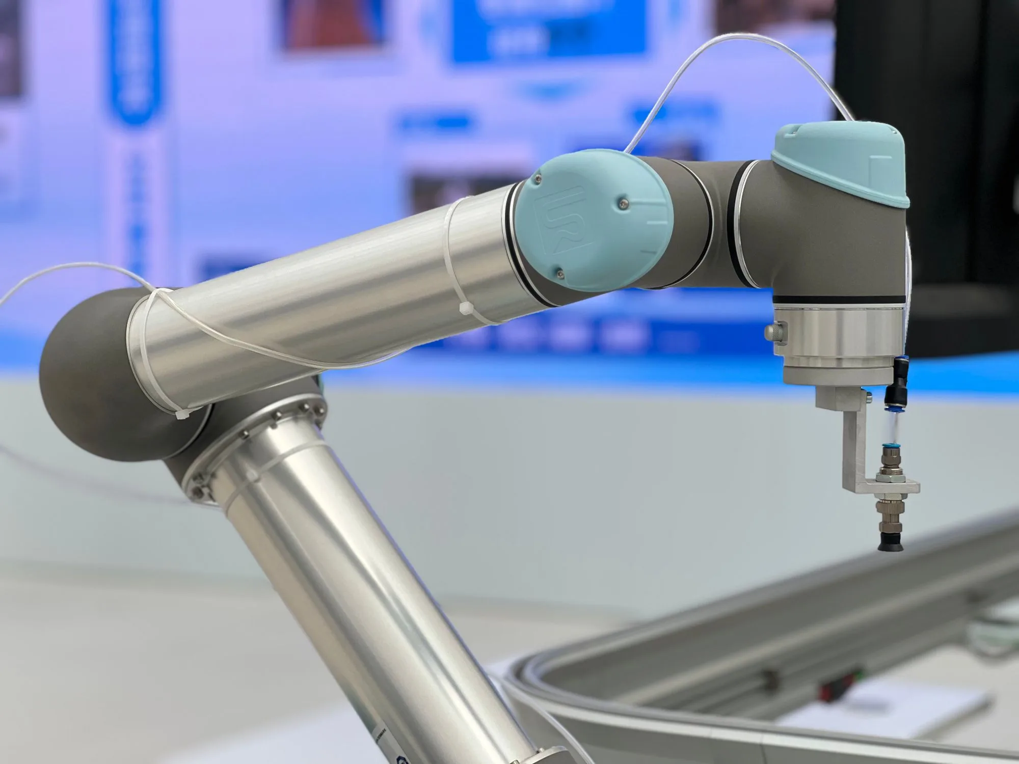
Once the design is validated on the bench, our electronic product design company runs a small pilot batch and puts the product through the same use it will see in the field. Issues that only surface at quantity get caught here, not at the customer's hand.
- In-house first-article assembly and inspection
- Test fixtures and bring-up scripts for the production line
- BOM lock with second sources and lifecycle checks
- Transfer to higher-volume manufacturing when the pilot says ready
Portfolio examples
Portfolio examples
Selected electronic product builds
A few of the electronic products our team has designed, prototyped, and helped manufacture. Tap any tile to open the full case study on lanpdt.com.
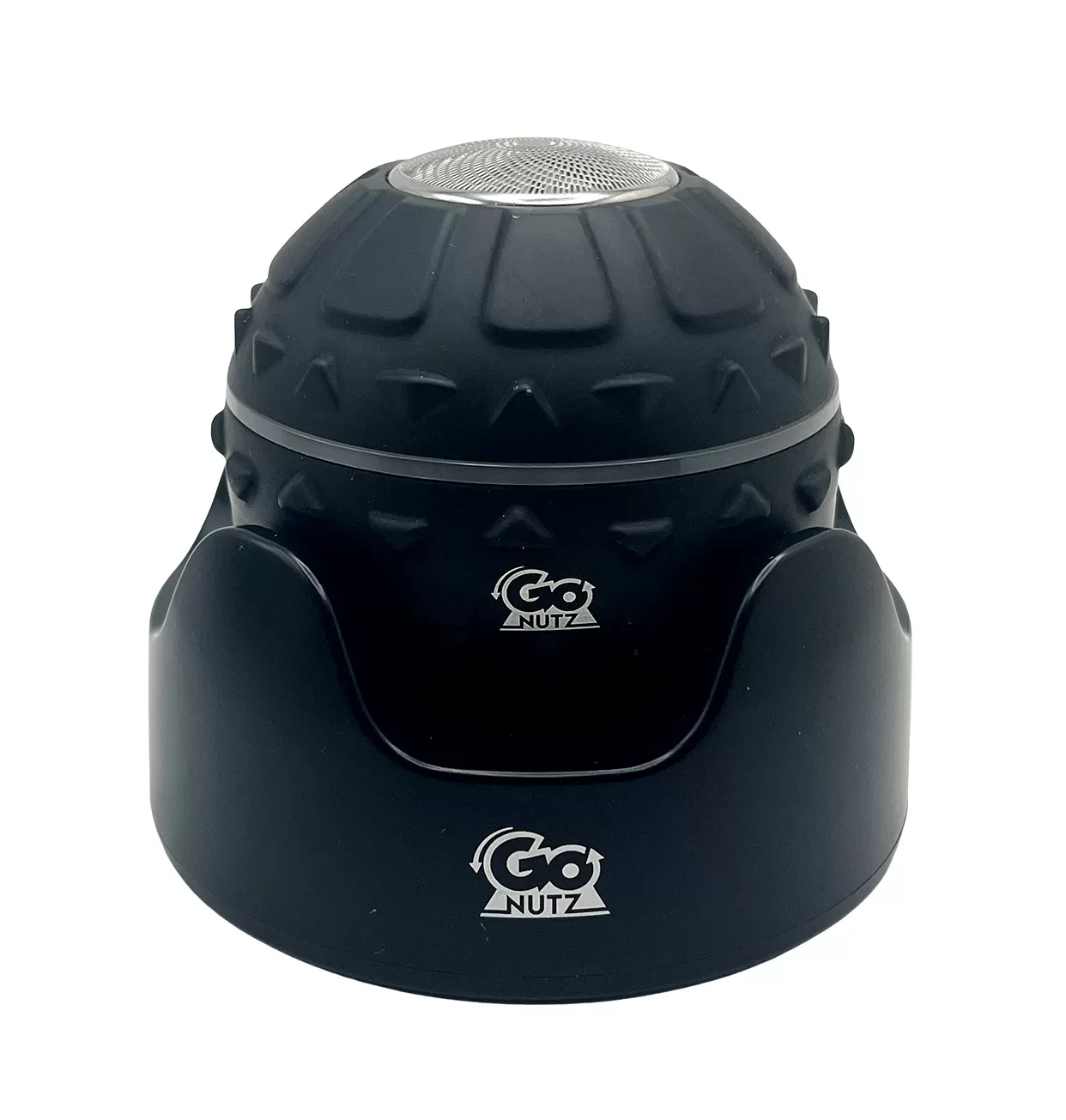
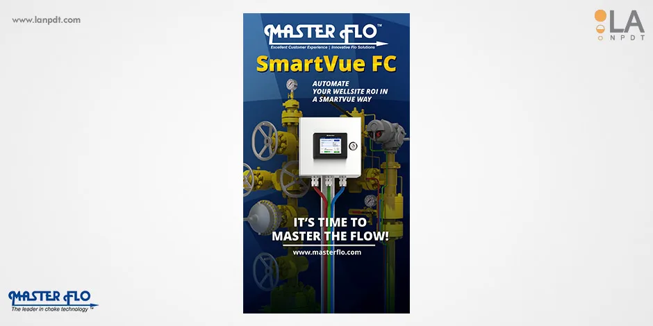
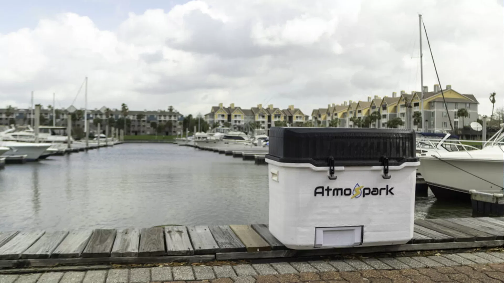
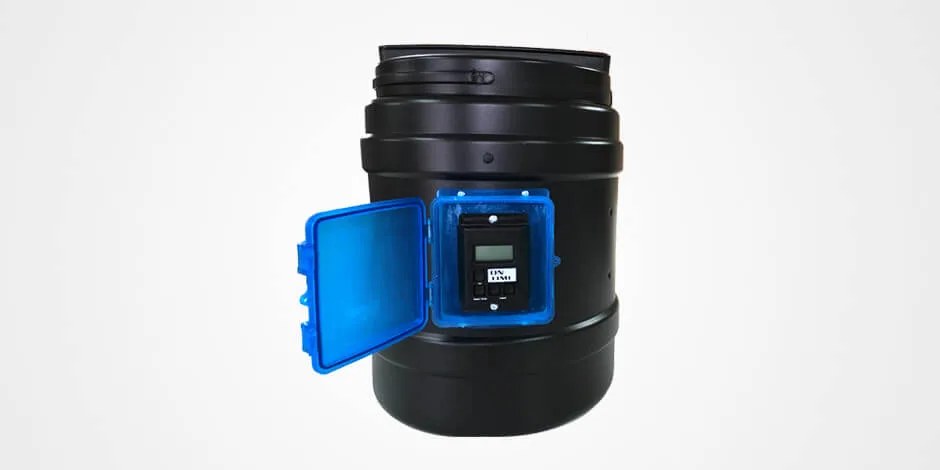
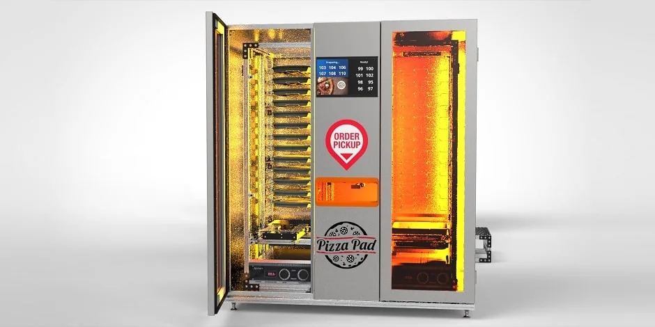
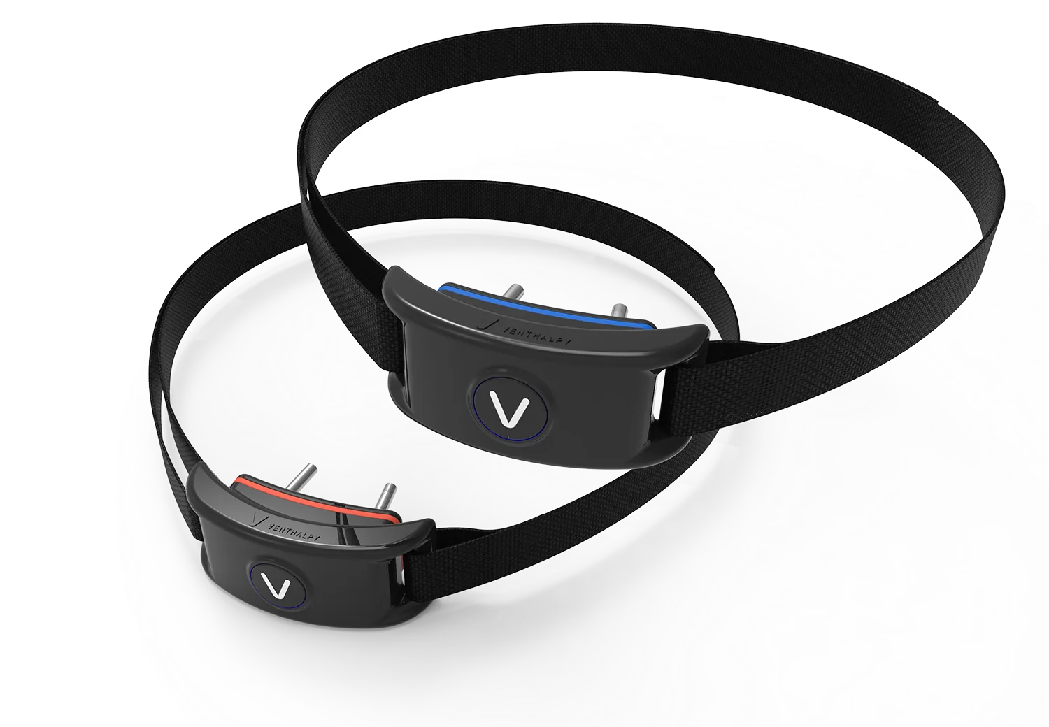
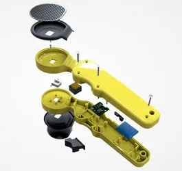
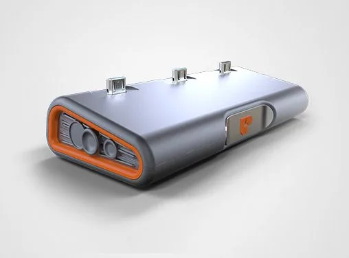
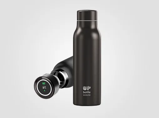
GoNutz Rechargeable battery system, electronics, prototyping Master Flo PCB enclosure design for SmartVue FC Atmospark Atmospheric water generator electronics Ontime Wildlife Feeders Electronic timer cover, prototypes & 3D print Bars Inc Automated pizza machine, control electronics & prototyping Venthalpy IoT HVAC efficiency wearable, custom PCB & iOS app UltraStrike Arc lighter PCB design and electronics prototyping Up Dock Multi-device charging hub, electronics & enclosure Up Bottle Smart water bottle with embedded temperature display
2015Operating since
1,000+Products developed
One teamSchematic → ship
In-houseLayout · firmware · pilot
Why it matters
- 01What good electronics design actually gets you
Done right, electronics design compresses the path from idea to a manufacturable product, and protects every dollar that follows in tooling, certification, and inventory.
- 02Faster decisions
A clear architecture and a tight BOM closes scope debates in days that would otherwise take months of back-and-forth between siloed vendors.
- 03Lower risk
Cheap kills before tooling. Component sourcing traps, RF surprises, and thermal misses get caught on the bench, not at the contract manufacturer.
- 04Scale-ready
The same team that drew the schematic walks it into pilot and volume production. One continuous chain, no rewrites at the factory door.
What clients say
What clients say
Electronics design that actually shipped
Words from founders, inventors, and product leads who hired our electronic product design company to get their hardware out of the bench and into the world.
ABOVE AND BEYOND! The team sets you up for success and will work creatively to assist you in your mission. A true pleasure to work with a company so good. I will be using them again in the future.

Jacob Penn Inventor & Entrepreneur
I could not be more pleased with the work of the team. Their professionalism, attention to detail, and methodical approach is nothing short of impressive. Every team member was just as excited about my project as I was.

Dr. Bob Cunningham CEO, Stir n Go
Amazing experience, by far the most professional, punctual, and talented designers I've come across. The words are not enough to describe the quality of the experience I've had with LA NPDT.

Catalina Park C&C Spectrum Innovation
Working with this company is so amazing. Very knowledgeable and accessible when needed. It is great to be able to work with people who are just as excited about your product as you are.

Brian Cooks Founder, Ziggo Sport
FAQ
FAQ
Frequently asked questions about our electronic product design company
- 01What does an electronic product design company actually do?
An electronic product design company handles schematic capture, PCB layout, firmware scoping, component selection against a target BOM, prototype build, bring-up, and DFM hand-off to short-run or volume manufacturing, all coordinated with mechanical and industrial design.
- 02Can you design the PCB and the enclosure together?
Yes. Our electrical, mechanical, and industrial design engineers sit on the same project. The board, the enclosure, and the user interface are scoped together so antennas, connectors, thermals, and mounting bosses do not collide late in the program.
- 03Do you handle low-volume PCB assembly and prototyping?
Yes. We build first-article prototypes in-house and run short-run assembly for pilot batches and crowdfunding fulfillment, then transfer to higher-volume manufacturing when the design is locked.
- 04What wireless and RF capabilities do you cover?
Bluetooth, BLE, Wi-Fi, LoRa, GSM/LTE modems, GPS, NFC, RFID, and antenna integration. We pick certified modules where it shortens compliance and lay out custom RF only when the product genuinely needs it.
- 05Do you write firmware?
We scope and write the firmware required to bring up the board, validate sensors and radios, and demonstrate the product. For deep application firmware we co-engineer with your team or a specialist partner under one program plan.
- 06How long does a typical electronics design engagement take?
A first working prototype usually lands in 8 to 14 weeks depending on RF, certification, and mechanical complexity. We scope the program in phases with a go / no-go decision after each, so cost and timeline stay under your control.
Need an electronic product design company for your hardware?
Schedule your free consultation and let's get to work. Bring the brief, we'll come back with an architecture, a BOM target, and a plan to a working prototype.
Electronics capabilities, specs and lead times
What an electronic product design company can actually do in house decides how long your project takes. Here is our scope, board by board.
| Capability | Specification | Typical lead time |
|---|---|---|
| Schematic capture | Analog, digital, mixed-signal; power budgets and part sourcing checked against real stock | 2–4 weeks |
| PCB layout | 2–12 layers, rigid, flex and rigid-flex; controlled impedance; IPC Class 2/3 | 2–5 weeks |
| Wireless | BLE, Wi-Fi, LTE-M/NB-IoT, LoRa, GPS/GNSS, NFC | Included in layout |
| Firmware | C/C++ on STM32, nRF52/53, ESP32, PIC; RTOS or bare metal; OTA update | 4–12 weeks |
| Power | Li-ion/LiPo charging and protection, buck/boost, low-power sleep budgeting | Included in schematic |
| Prototype assembly | In-house bring-up, rework and test of first articles | 1–2 weeks after fab |
| Compliance preparation | Pre-scan for FCC Part 15, CE, and design for UL/IEC where required | 2–6 weeks |
| Production handoff | Gerbers, BOM, pick-and-place, test fixtures, DFM review with the assembler | 1–3 weeks |
What you receive
- Schematics and a costed bill of materials with sourced, in-stock parts and second sources.
- PCB layout files, Gerbers, pick-and-place and fabrication drawings — all yours.
- Firmware source, build instructions and a documented flashing procedure.
- Assembled and bring-up-tested prototype boards, with a test report of what passed.
- A compliance readiness note listing what an accredited lab will still need to certify.
Cost and turnaround ranges
| Scope | Typical cost | Typical turnaround |
|---|---|---|
| Simple sensor or controller board, no wireless | $8,000–$20,000 | 6–10 weeks |
| Connected product: MCU, BLE or Wi-Fi, battery, firmware | $25,000–$75,000 | 12–20 weeks |
| Cellular or GNSS wearable with power management | $45,000–$120,000 | 16–28 weeks |
| Layout only, from your schematic | $3,000–$12,000 | 2–5 weeks |
| Firmware only, on existing hardware | $10,000–$40,000 | 6–14 weeks |
Certification testing at an accredited lab is a separate cost, usually $8,000–$25,000 depending on radios and markets. We design for it rather than hoping for it, which is what keeps most projects to a single lab visit.
Design-only studio vs full-service engineering
| Capability | Design-only studio | LA NPDT |
|---|---|---|
| Schematic and layout | Often subcontracted | In house |
| Firmware | Separate vendor | Same team as the hardware |
| Enclosure and mechanical fit | Handled by another partner | Designed alongside the board |
| Prototype build and bring-up | Shipped out | In-house prototyping |
| First production run | Your problem | Short-run manufacturing |
Recent electronics projects
- GPS tracking bracelet — GNSS, cellular and battery management in a wearable form factor.
- SmartVue PCB and enclosure design — board and housing engineered together.
- PCB design projects — a cross-section of boards we have taken from schematic to assembly.
Frequently Asked Questions
- 01How much does electronic product design cost?
A simple non-wireless board is $8,000–$20,000. A connected product with an MCU, radio, battery and firmware typically runs $25,000–$75,000, and a cellular or GNSS wearable can reach $120,000. Layout-only and firmware-only engagements are much smaller.
- 02How long does PCB design and firmware take?
Schematic and layout take four to nine weeks together. Firmware overlaps and adds four to twelve weeks. Plan on twelve to twenty weeks from kickoff to a working, bring-up-tested connected prototype.
- 03Do you handle FCC and CE certification?
We design for compliance, run pre-scans and prepare the documentation, then work with an accredited lab that issues the certification. We manage that process with you; the lab issues the certificate.
- 04Can you work from an existing board or a dev-kit prototype?
Yes. Bringing a dev-kit build to a custom board is one of the most common projects we take — we keep the proven behavior and re-engineer the hardware for size, cost and power.
- 05Who owns the schematics, layout and firmware?
You own all of it: source files, Gerbers, BOM and firmware, delivered at the end of the project under NDA from day one.
- 06Can you design the enclosure too?
Yes. Mechanical and electronic engineering sit in the same team, so the board is laid out around the housing and the housing around the board, instead of one being forced to fit the other later.
When electronics need a sealed silicone overmold or flexible wearable band, see our silicone rubber prototyping and manufacturing hub.
How an electronics program actually runs
Hardware fails on schedule far more often than on physics. These are the five stages we run, what gets decided in each, and the thing that most often goes wrong when a stage is skipped.
| Stage | What you get | Typical duration | What goes wrong if it is skipped |
|---|---|---|---|
| Requirements and architecture | Block diagram, power budget, interface list, risk register | 1-2 weeks | Scope creep lands mid-layout, when every change costs a board spin |
| Schematic and part selection | Reviewed schematic, bill of materials with second sources, lifecycle check | 2-3 weeks | The design freezes around a part with 40-week lead time |
| PCB layout and DFM | Layout, stackup, gerbers, assembly drawings, fab house review | 2-3 weeks | Boards fabricate fine and assemble badly, or fail EMC on trace routing |
| Bring-up and firmware | Working prototypes, firmware, test procedures, measured performance | 3-5 weeks | Hardware bugs surface as firmware bugs and burn weeks of debug |
| Pre-compliance and handoff | Pre-scan results, corrected design, production package | 2-4 weeks | The first paid lab visit fails and the schedule slips a month |
Electronics rarely ships alone. The board has to fit an enclosure, survive drop and heat, and be assembled at a price. That work runs in parallel with industrial design and mechanical CAD, then hands to low-volume manufacturing with one bill of materials rather than three.
Electronic design questions we get asked
What does an electronic design engagement include?
Requirements and architecture, schematic capture, PCB layout, component selection with second sources, design for manufacture and test, firmware, bring-up of the first boards, and the certification path. You leave with the schematics, layout files, bill of materials, firmware source and test procedures in your name.
How much does a custom PCB design cost?
A simple sensor or control board with an existing reference design typically runs $8,000 to $20,000 through first working prototypes. A connected product with wireless, power management and a custom enclosure interface usually lands between $25,000 and $70,000.
Multi-board systems, safety-critical devices and anything needing intrinsic safety or medical documentation go past that. Board fabrication and assembly for a prototype run are separate and usually $1,500 to $8,000.
How long does it take to get a working board?
Four to eight weeks from a settled requirements document to a bring-up-ready prototype for a straightforward board, assuming parts are in stock. Wireless products add two to four weeks for antenna tuning and pre-compliance. Most programs run two spins before the design is frozen; budgeting for a third avoids schedule panic.
Do you handle FCC, CE and UL certification?
We design for it and run the program. That means pre-compliance scans on our own bench before anything goes to a lab, a documented test plan, and coordinating the accredited lab that issues the certificate. Certification bodies issue the marks; we make sure the hardware passes the first time instead of paying for repeat lab days.
Can you design around parts that are actually available?
Yes, and it is a design constraint from day one. Every critical component is checked for lifecycle status and stock depth, and second sources are picked before layout so a footprint can accept an alternate. Boards laid out around a single sole-sourced part are the most common reason a working prototype cannot be built in volume.
Who owns the firmware and design files?
You do. Schematics, layout, gerbers, bill of materials, firmware source and test fixtures transfer to you at the end of the engagement, and there is no license back to us. That also means you can take the package to any contract manufacturer instead of being locked to ours.
Related services
- Digital product development services
When the board needs firmware, a cloud back end and an app around it.
What founders say after working with us
“Konstantin has been so amazing and his entire team is A+. I researched and interviewed many product development companies across the country and ultimately decided on LA NPDT... and I'm so glad I did. The attention to detail and overall effort has been exactly what I needed and then some. If you are looking for a company to help you bring your product to life, look no further!”
 William EvansCEO, Burple
“This company is awesome. I run a medical device company and we required a number of accessories to be designed and built for our medical device. They delivered a polished design and printed the accessories on time using high-quality materials. I continue to work with them for all of our material needs.”
 Matteo ZiffFounder, Virtual Vision
“Partnering with LA NPDT to bring LEIA to life was a game-changer. Their blend of market analysis, design expertise, prototyping, and manufacturing streamlined my vision into a tangible solution. For medical professionals with a product idea, there's no team I'd recommend more.”
 Dr. Elena DolganFounder, LEIA Cup
Three reasons founders keep working with us
- 1
One team from sketch to shipped parts. Industrial design, mechanical and electrical engineering, prototyping and manufacturing sit under one roof, so nothing is lost in a handoff.
- 2
You own the work. Native CAD, drawings and source files are yours at the end of every phase — no lock-in, no re-buying your own design later.
- 3
Fixed scope, fixed price. Every phase is quoted up front with a deliverable list and a date. No hourly meters, no surprise invoices.
If you ever thought of developing a new product, don’t wait any longer. Talk with one of our experts today.
Tell us about your product
Send us the idea, the drawing or the problem. We reply within one business day with the next practical step.
Ready to scope the work? Get engineering support · Request a quote