Electronic Product Development: How to Approach It
Electronic product development follows six stages from requirements to design transfer. Here is what happens in each, what it costs, and the mistakes that force expensive board revisions.
November 28, 20228 min read

Written by Konstantin Dolgan, Ph.D., NPDP
Founder & CEO, Product Development Engineer
Published November 28, 2022Updated September 2, 2026
Electronic product development is the process of turning a functional concept into manufacturable hardware: defining requirements and architecture, designing the schematic, laying out the PCB, writing and bringing up firmware, passing EMC and safety testing, and transferring the design to a manufacturer. Most programs need two to three board revisions before production.
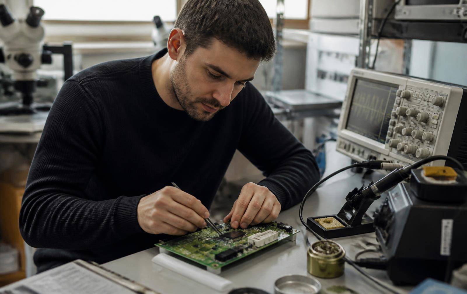
Electronics fail differently from mechanical parts. A mechanical mistake usually shows up as a fit problem you can see. An electronics mistake shows up as intermittent behavior at temperature, a failed emissions scan, or a component that goes end-of-life two months before launch. The stages below are organized to surface those failures early.
Stage 1: Requirements and architecture
Before any schematic, write down what the device must do in measurable terms: power source and budget, connectivity, sensors and actuators, environmental conditions, expected lifetime, target cost and the markets it will be sold in. Market list matters immediately because it determines which certifications apply.
- Power budget: current draw per mode and required runtime — this drives nearly every downstream choice.
- Connectivity: BLE, Wi-Fi, cellular or wired, and whether a pre-certified module removes radio testing burden.
- Processing: the smallest MCU that comfortably meets the need, with headroom for firmware growth.
- Environment: temperature range, ingress, vibration, ESD exposure.
- Cost target: a BOM ceiling derived from the retail price and channel margin.
Stage 2: Schematic design
The schematic defines the circuit: power regulation, processor, memory, radios, sensors, protection and connectors. Component selection at this stage is a supply chain decision as much as an engineering one — choose parts with multiple sources, long lifecycle status and real availability, not just the best datasheet.
Decision | Why it matters later |
|---|---|
MCU family | Toolchain, firmware portability, and second-source options |
Pre-certified radio module vs discrete | Module cuts weeks and thousands from radio certification |
Power topology | Efficiency, thermals, and EMI behavior |
Protection (ESD, reverse polarity, overcurrent) | Field failures and warranty cost |
Test points and debug header | Whether the factory can test the board at all |
Stage 3: PCB layout
Layout is where a correct schematic becomes a working or failing product. Placement determines thermal behavior, trace routing determines signal integrity, and ground strategy largely determines whether the board passes EMC on the first attempt.
- Set the mechanical envelope first — board outline, connector positions and mounting holes come from the enclosure CAD.
- Keep switching regulators and their loops tight, away from analog and antenna areas.
- Follow the module vendor's antenna keep-out and reference layout exactly.
- Design for assembly: consistent component orientation, adequate spacing, fiducials, and panelization discussed with the manufacturer.
Stage 4: Firmware and bring-up
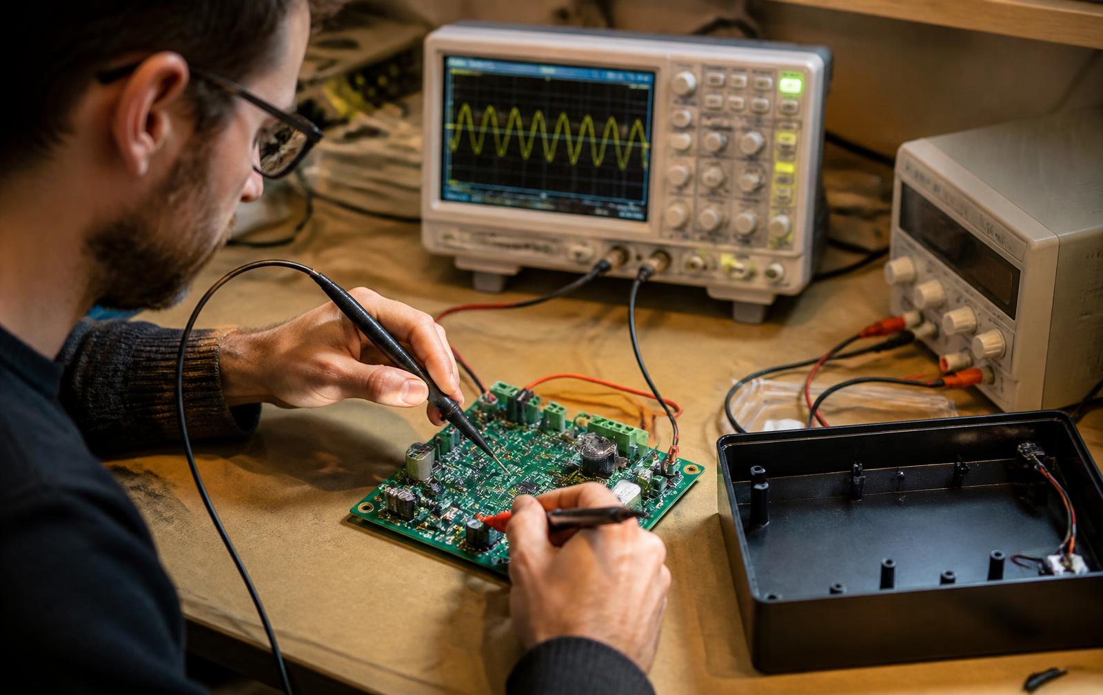
Bring-up is the first time hardware and firmware meet. Plan it as a sequence — power rails, clocks, debug interface, then peripherals one at a time — and keep a written log of every deviation. Budget real time here; teams routinely underestimate bring-up by half.
- Verify rails and current draw against the power budget before running any application code.
- Bring up the debug interface and a serial console first — everything else depends on visibility.
- Enable peripherals individually, confirming each against a known-good reference.
- Add a production test firmware image early; the factory needs it, not the application build.
- Build in a field-update path before launch, not after the first bug report.
Stage 5: EMC, safety and compliance testing
Certification is a schedule risk, not a formality. Emissions and immunity failures usually require layout changes, which means a board respin and often an enclosure change. Pre-scan at an accredited lab as soon as an integrated prototype exists — a half-day pre-compliance session is far cheaper than a failed formal test.
Requirement | Applies to | Typical cost |
|---|---|---|
FCC Part 15 (US) | Any device with a digital clock or radio | $5,000 to $20,000 |
CE / UKCA (EU, UK) | Products sold in those markets | $5,000 to $25,000 |
Radio module certification | Reduced significantly if using a pre-certified module | $0 to $15,000 |
Safety (UL, IEC 62368/60601) | Mains-powered, medical or high-energy devices | $10,000 to $75,000+ |
Battery (UN 38.3, IEC 62133) | Any lithium cell product that ships | $3,000 to $15,000 |
Stage 6: Design transfer to manufacturing
Design transfer is a documentation package, not an email with Gerbers. It includes fabrication and assembly files, a fully specified BOM with approved manufacturer part numbers and alternates, assembly drawings, test procedures and acceptance criteria, and the production test firmware. Choosing the right partner matters as much as the package — see our guide to selecting an electronics contract manufacturer.
Realistic budgets and timelines
Product complexity | Engineering cost | Timeline to production |
|---|---|---|
Simple sensor or accessory, pre-certified module | $25,000 to $60,000 | 4 to 7 months |
Connected consumer device with app | $60,000 to $180,000 | 8 to 14 months |
Industrial or safety-certified device | $150,000 to $400,000+ | 14 to 30 months |
These exclude tooling and certification. For how electronics fits into the wider program, see the new product development process.
The five most expensive mistakes
- Selecting components without checking lifecycle and availability. An end-of-life part after layout means a respin.
- Leaving EMC to the end. A late emissions failure costs a board revision plus lab re-booking.
- No production test strategy. Untestable boards produce field failures the factory could have caught.
- Designing the PCB before the enclosure. Mechanical constraints always win, and rerouting is the cheaper of the two changes.
- Budgeting one board revision. Two to three is normal; pretending otherwise just moves the overrun to the schedule.
Frequently asked questions
What is electronic product development?
Electronic product development is the end-to-end process of turning a functional concept into manufacturable electronic hardware. It covers requirements and architecture, schematic design, PCB layout, firmware development and bring-up, EMC and safety compliance testing, and design transfer to a contract manufacturer.
How much does it cost to develop an electronic product?
A simple accessory using a pre-certified module typically costs $25,000 to $60,000 in engineering. A connected consumer device with a companion app usually runs $60,000 to $180,000, and industrial or safety-certified products $150,000 to $400,000 or more, excluding tooling and certification fees.
How long does electronic product development take?
Four to seven months for a simple device, eight to fourteen months for a connected consumer product, and fourteen to thirty months for industrial or medical hardware where safety certification dominates the schedule.
How many PCB revisions should I expect?
Two to three revisions before production is normal. The first board proves the architecture, the second fixes bring-up findings and EMC issues, and the third is production-intent. Budgeting for only one revision is the most common cause of schedule overrun.
Should I use a pre-certified radio module?
For most products, yes. A pre-certified module removes the majority of radio certification cost and risk, shortens the schedule by weeks, and avoids antenna tuning work. Discrete radio designs make sense mainly at high volume where the per-unit saving outweighs the certification investment.
When should compliance testing start?
Compliance planning starts at stage one, when you decide which markets the product will sell in. Physical pre-compliance scanning should happen as soon as an integrated prototype exists — well before design freeze — because emissions failures usually require layout changes.
Component sourcing is a design decision
Schematics get judged on function; bills of materials get judged on availability. A design that specifies a single-source MCU with a 40-week lead time is not finished, no matter how elegant the circuit. Run a sourcing review at schematic freeze and again before layout release, and treat lifecycle status as a hard requirement alongside electrical specifications.
BOM risk review criteria
Risk factor | Acceptable | Needs mitigation |
|---|---|---|
Lifecycle status | Active, with a published longevity commitment | NRND or last-time-buy notice |
Sources | Two or more qualified alternates | Single source, no drop-in equivalent |
Lead time | Under 16 weeks | Over 26 weeks |
Minimum order quantity | Matches your first production run | Reels far above annual usage |
Package availability | Standard, multiple package options | Single unusual package |
Certification impact | Pre-certified module or known-good part | Custom radio requiring full testing |
Layout for substitution where you can: footprints that accept two regulator families, a pin-compatible memory alternate, and passives at common values rather than exotic ones. Each of those choices costs nothing at design time and can save a respin when a part goes unavailable mid-ramp.
Sourcing checklist at layout release
- Every line item has a lifecycle status and a named alternate, or a documented reason it does not.
- Quotes reflect your actual build quantity, not a distributor's single-unit price.
- Long-lead parts are ordered against the build schedule, not after the boards arrive.
- Radio modules are pre-certified where certification budget is tight.
- A last-time-buy plan exists for anything already flagged NRND.
Key takeaways
- Availability and lifecycle belong in the schematic review, not the purchasing stage.
- Design footprints that accept alternates; substitution is cheaper than a respin.
- Order long-lead parts against the build schedule, not after layout.
Electronics and enclosure have to be designed together
The most common structural failure in electronic product development is organisational: the board is designed by one group, the housing by another, and they meet at the first assembly. By then the connector is 3 mm from where the opening is, the antenna sits behind a metal bracket, and the only remaining fix is a board revision.
Interface | Decide by | Failure if left late |
|---|---|---|
Board outline and mounting holes | Before layout starts | Full re-layout, four to six weeks lost |
Connector and button positions | Before layout starts | Openings that do not line up, or hand-fitted gaskets |
Antenna keep-out and ground plane | Before layout starts | Range loss that no firmware change recovers |
Thermal path from regulators and processor | Before layout release | Throttling, or a fan added to a product designed to be silent |
Display bonding and light guides | Before the first enclosure tool | Visible light leak, uneven backlight, cosmetic rejects |
Service and battery access | Before the first enclosure tool | Returns that cannot be repaired economically |
The practical fix is a shared mechanical-electrical model reviewed weekly during layout: a STEP export of the board into the enclosure model, and the enclosure back into the ECAD tool. It takes an hour a week and removes the most expensive revision in the program.
Planning bring-up and test equipment
Bring-up is scheduled optimistically almost every time. Budget two to three weeks for a first board of moderate complexity, and make sure the tools and access points exist before the boards arrive.
- Test points on every rail and on the reset, boot and debug lines — probing a 0402 pad is a fifteen-minute job that should have been a two-second one.
- A debug header that survives to production, even if it is depopulated; field diagnosis depends on it.
- Current-sense provision in the power path, so the power budget can be measured rather than estimated.
- Bootloader and recovery path decided at design time, not after the first bricked unit.
- A written bring-up sequence — rails, clocks, memory, radio, peripherals, application — so failures are isolated rather than guessed at.
Production test at the contract manufacturer
Every unit needs a pass or fail decision on the line, and that decision needs a fixture. Plan for it during layout: a bed-of-nails fixture needs test pads on a 2.54 mm-friendly grid on one side of the board, plus tooling holes for alignment. Retrofitting test access after design release is a board revision and a schedule slip.
Test stage | What it catches | Typical cost |
|---|---|---|
Automated optical inspection | Placement, polarity and solder defects | Included by most contract manufacturers above a few hundred units |
In-circuit or flying probe test | Shorts, opens, wrong values | $3,000 to $12,000 fixture, or per-board flying probe fees |
Functional test fixture | Firmware load, radio check, sensor calibration | $5,000 to $25,000 to design and build |
Burn-in or run-in | Infant mortality in power components | Line time, typically pennies to a dollar per unit |
Key takeaways
- Mechanical and electrical design have to share a model from the first day of layout.
- Design bring-up access into the board; it is unrecoverable later.
- Certification and production test are schedule items, not paperwork at the end.
- Two to three board revisions before production is normal — plan and fund them.
Firmware does not stop at launch
Mechanical products ship and are finished. Electronic products ship and start accruing obligations: security patches, protocol changes at the cloud provider, phone operating systems that deprecate a Bluetooth behaviour, and the bugs that only appear across ten thousand units. Budget for that from the beginning rather than discovering it in the second year.
- Decide the update path at architecture stage: over-the-air, app-mediated, USB, or none at all — each choice sizes the flash memory you need to specify now.
- Reserve memory for dual-bank updates, so a failed update falls back instead of bricking a unit in a customer kitchen.
- Sign firmware images and verify the signature on device; an unsigned update path is a recall waiting to happen.
- Plan a staged rollout — one percent of the fleet, then ten, then all — with a metric that stops the rollout automatically.
- Budget engineering time after launch: ten to twenty percent of the original firmware effort per year is a realistic maintenance figure.
The same discipline applies to the hardware side. Keep the bill of materials under review after launch, because component obsolescence does not pause for your production schedule, and a last-time-buy notice with a six-week response window is far easier to handle when an alternate part has already been qualified.
Planning an electronics program and worried about sourcing risk?
Work with LA NPDT: if you are moving from here to execution, start with our our product development process or talk to us about end-to-end product development.
Filed under:EducationInspirationWords
Services related to this guide
- Electronic design servicesSchematic, PCB layout, firmware and bring-up, through to production handoff.
- Rapid prototypingWorking prototypes in days, from 3D printing to vacuum casting.
- Product design servicesIndustrial design and CAD taken all the way to manufacturable files.
- Product development examplesReal projects we designed, prototyped and shipped.