Written by Ashok Chintagunta, MS Computer Science, Louisiana Tech University
CTO & Software Engineer, AI and Automation
Published August 10, 2026
A PCB design company lays out your circuit board so it works electrically, fits the enclosure, and can actually be assembled — three constraints that fight each other.
On this project we took a client's schematic into a production layout: component placement, routing, stack-up, and Gerber files a board house could fabricate and assemble from.
Project at a glance
- Category
- Electronics / PCB layout
- What we delivered
- Schematic review, PCB layout, Gerber and assembly package
The client

The challenge
Our solution
The result
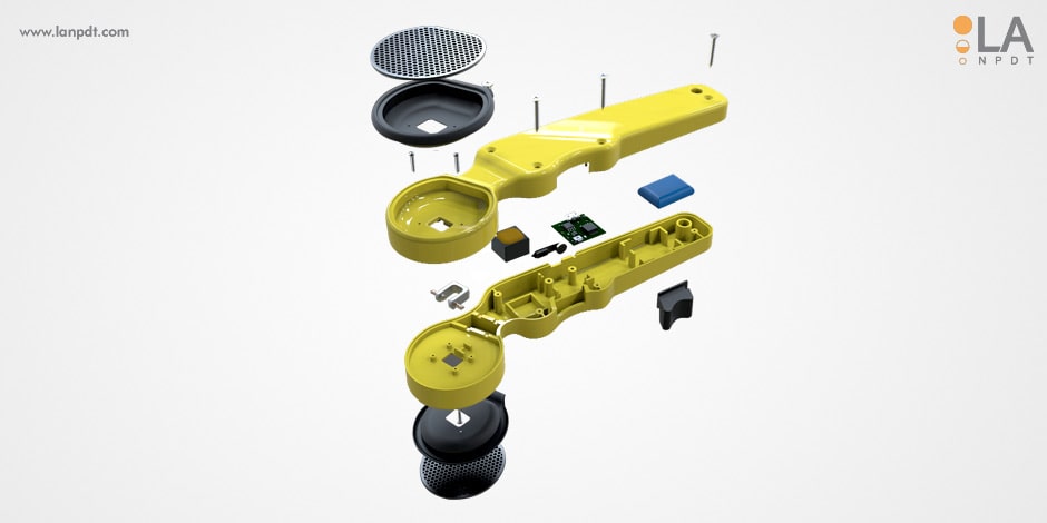
PCB design project at a glance
| Scope | Schematic capture, multilayer PCB layout, BOM, prototype boards |
|---|---|
| Typical stack | Microcontroller, power regulation, sensors, wireless connectivity |
| Deliverables | Schematics, Gerbers, BOM, assembly drawings, tested prototype |
| Typical timeline | 4-10 weeks from requirements to a tested board |
What a PCB design company is responsible for
The board is where cost, size, battery life and reliability are decided. That means selecting parts that will still be available in two years, laying out power and ground so the device passes EMC, keeping analog away from switching noise, and leaving room for the test points that make debugging possible.
Our process
- Requirements first: power budget, interfaces, size envelope, certification targets
- Architecture and part selection against availability and lifecycle
- Schematic capture with review before layout begins
- Layout with attention to stack-up, return paths and thermal relief
- Prototype build, bring-up and firmware validation on real hardware
Frequently asked questions
How much does PCB design cost?
A simple two-layer board typically runs $2,000-$6,000; a multilayer board with wireless and mixed-signal sections generally runs $10,000-$40,000 including bring-up.
Do you also write firmware?
Yes. Firmware, bring-up and test scripts are handled by the same team that designs the board.
Can you design the enclosure around the board?
Yes - mechanical and electrical are developed together, which avoids the usual late-stage fight over connector positions.
Capabilities used on this project
Electronic design and PCB engineering
Schematic capture, PCB layout, firmware and electromechanical integration for connected hardware.
Rapid prototyping services
3D printing, CNC machining, urethane casting and functional prototype builds with published materials, tolerances and lead times.
Low-volume manufacturing
Bridge tooling, short-run production and supplier management for first commercial batches.
How a PCB goes from schematic to production
1. Start from a verified schematic
Layout cannot fix a broken circuit. We review the schematic against the product requirements first, because a layout change costs hours and a circuit change after boards are ordered costs a respin.
2. Place components for the enclosure, not just the circuit
Connectors, LEDs and buttons have to land where the industrial design puts the holes. We place against the mechanical model so the board and housing converge instead of colliding.
3. Route for signal integrity and assembly
Power planes, controlled impedance where needed, and footprints the assembler can actually populate. A board that routes beautifully but cannot be machine-assembled is an expensive prototype.
4. Release a complete fabrication package
Gerbers, drill files, pick-and-place, BOM with approved alternates, and assembly drawings. Board houses quote and build exactly what you release — nothing more.
| Decision | Lower cost | Higher cost |
|---|---|---|
| Layers | 2-layer board | 4+ layers with blind vias |
| Components | Standard packages | Fine-pitch BGA, flex sections |
| Assembly | SMT one side | Double-sided, mixed through-hole |
| Compliance | No certification needed | FCC / UL pre-compliance design |
Questions about this project
Straight answers from the engineers who ran the build. Have a different question? Ask us directly.
Talk to an engineerHow much does PCB design cost?
A straightforward 2–4 layer board typically runs $3,000 to $12,000 in layout and release work, depending on component count and constraints. Prototype boards and assembly are quoted separately per quantity.
I only have an idea, not a schematic — where do I start?
With the product requirements. We develop the circuit architecture, draw the schematic, then lay out the board — you do not need to arrive with engineering already done.
How long does a PCB layout take?
Simple boards route in one to two weeks; dense multilayer designs take longer. Add two to four weeks for fabrication and assembly of the first articles.
Industries this project belongs to
See how we approach development in each of these categories, and the other products we have taken from sketch to production there.