PCB Assembly Process: From EVT Boards to Mass Production
Architecture, layout, EVT, DVT and PVT explained, with what each build stage costs and how long it takes to reach production.
December 17, 20195 min read

Written by Konstantin Dolgan, Ph.D., NPDP
Founder & CEO, Product Development Engineer
Published December 17, 2019Updated September 2, 2026
The PCB assembly process is where an electronics design stops being a schematic and starts being a yield number. Stencil, paste, pick-and-place, reflow, inspection and functional test each add cost and each fail differently at EVT, DVT and PVT volumes. Skipping a build stage does not save time; it moves the failure later, where a fix costs ten times more.

What each stage answers
- Architecture - can this be built at the target cost and power budget? Output is a block diagram, a costed BOM and a risk list.
- Schematic and PCB layout - does the design close electrically, thermally and mechanically inside the enclosure? Output is a fabrication and assembly package.
- EVT (engineering validation) - does it work at all? Bring-up, functional test, and honest measurement against spec on 5-20 units.
- DVT (design validation) - does it work reliably and legally? Environmental, drop, life testing and pre-compliance scans on 50-200 units.
- PVT and mass production - can the factory build it repeatably? Pilot run on production tooling with real operators, fixtures and yield data.
Costs by stage
Stage | Typical duration | Engineering cost | Build cost |
|---|---|---|---|
Architecture | 3-5 weeks | $12,000-$35,000 | - |
Schematic and PCB layout | 6-10 weeks | $35,000-$90,000 | $3,000-$12,000 |
EVT | 4-6 weeks | $20,000-$50,000 | $8,000-$25,000 |
DVT | 6-10 weeks | $30,000-$80,000 | $25,000-$80,000 |
Certification | 6-12 weeks | $5,000-$20,000 support | $15,000-$60,000 lab |
PVT and ramp | 4-8 weeks | $15,000-$45,000 | Tooling plus pilot units |
Where electronics schedules slip
- Component availability. Design around parts with real lead times and approve second sources at schematic, not at PVT.
- Certification surprises. Run pre-compliance during DVT; discovering radiated emissions failures at the lab costs a full spin.
- Mechanical-electrical collisions. Enclosure and PCB must be reviewed together at every layout revision.
- Firmware treated as parallel and free. Bring-up needs firmware ready when boards land, or EVT stalls.
- No test fixtures. A factory cannot test what you did not design a fixture for; budget it during DVT.
What to have before you start
A written requirements document with power budget, target cost, environment and regulatory market list beats a pile of feature ideas. Bring that and a rough industrial design intent, and architecture takes weeks instead of months. See our electronic design services and low volume manufacturing for how we run these stages together.
PCB assembly quote line items
Line item | Prototype (10 pcs) | Pilot (500 pcs) | Notes |
|---|---|---|---|
Bare boards | $25-$90 ea | $3-$12 ea | Panelization cuts this sharply |
Stencil | $100-$250 | Amortized | One per board revision |
NRE and programming | $300-$1,200 | $300-$1,200 | Per assembly setup |
SMT placement | $1.50-$4.00 ea | $0.30-$1.20 ea | Driven by placement count |
Through-hole and hand work | $8-$40 ea | $2-$10 ea | Eliminate where possible |
Functional test | $10-$60 ea | $1.50-$8 ea | Requires a fixture you must fund |
Assembly-ready data package
- Gerbers or ODB++ with a fabrication drawing specifying stackup, finish and impedance.
- Centroid / pick-and-place file with consistent rotation conventions.
- BOM with manufacturer part numbers and approved alternates. Generic descriptions cause substitutions you did not approve.
- Assembly drawing with polarity and first-article notes. Diodes and connectors are the usual reversals.
- Test procedure and pass criteria. Without it, the CM only verifies solder joints, not function.
- Firmware image and programming instructions, including how serial numbers are assigned.
EVT, DVT and PVT builds for electronics
PCB assembly maturity is described in three builds. EVT proves the circuit works: small quantities, hand-placed rework expected, and a schedule measured in weeks. DVT proves the design is manufacturable and passes testing: production-intent stackup, real components, pre-compliance runs. PVT proves the factory can build it repeatably at rate, with test fixtures, yield data and process documentation in place.
Compressing these builds is the most common cause of a stalled hardware launch. A board that skips DVT arrives at PVT with unqualified components and no test coverage, and the factory discovers problems while burning line time you are paying for.
Build | Quantity | Assembly cost per unit | Purpose |
|---|---|---|---|
EVT | 5-25 | $150-$600 | Prove function, find design errors |
DVT | 50-250 | $60-$200 | Prove manufacturability and compliance |
PVT | 250-2,000 | $20-$80 | Prove yield and process at rate |
Mass production | 2,000+ | $8-$40 | Sustained output |
Design for assembly and test coverage
Assembly cost and yield are set at layout. Single-sided placement avoids a second reflow pass. Consistent component orientation speeds placement and inspection. Fiducials, adequate courtyard spacing and standard package sizes let the pick-and-place run at full speed. Test points and a boundary-scan or ICT strategy determine whether a defective board can be diagnosed in seconds or gets scrapped.
Agree the test strategy with the contract manufacturer during DVT, not after. A functional test fixture is a small tooling project of its own - typically $3,000 to $15,000 - and building it late means PVT ships untested boards.
- Keep components on one side where volume allows to avoid a second reflow.
- Use standard package sizes; exotic parts slow the line and raise cost.
- Add fiducials and respect courtyard spacing for automated placement.
- Design in test points and define pass/fail limits early.
- Qualify a second source for every critical component.
- Budget and schedule the functional test fixture during DVT.
The PCB assembly process, stage by stage
PCB assembly looks like one operation on a quote and is really six. Knowing the sequence helps you read a quote, understand where cost sits, and design boards that do not fight the line.
Stage | What happens | Cost driver | Where designs cause trouble |
|---|---|---|---|
Solder paste printing | Stencil deposits paste on pads | Stencil cost, one-time | Odd pad geometry, no fiducials |
Pick and place | Machine places SMT components | Placement count, feeder setups | Too many unique part numbers |
Reflow | Oven profile melts solder | Profile development | Mixed thermal mass, large ground planes |
Inspection (AOI / X-ray) | Automated optical, X-ray for BGA | Board complexity | No test points, hidden joints |
Through-hole and selective solder | Connectors and headers | Manual labor | Mixing THT into an SMT-only quote |
Test and depanel | Functional test, routing | Fixture build | No boundary scan or test access |
Design choices that lower assembly cost
- Single-sided placement when possible — a second reflow pass adds setup and risk.
- Consolidate part numbers. Ten resistor values cost less to set up than twenty-five.
- Add fiducials and tooling holes; without them the panel needs manual alignment.
- Panelize deliberately with the assembler's preferred array and rail width.
- Provide test points on power rails, communication lines and reset — retrofitting them is painful.
- Specify approved alternates in the BOM so a shortage does not stop the line while you decide.
Boards designed against the assembler process rules typically quote 15–30 percent lower and reach stable yield sooner — that review is part of our electronic design services.
Key takeaways
- EVT, DVT and PVT each answer a different question - do not skip one.
- Assembly cost is largely determined by layout decisions.
- Test strategy and fixtures must be built during DVT, not at production.
- Second-source critical components before they go end-of-life.
- Yield data from PVT is what makes a production quote credible.
Working with a contract electronics manufacturer
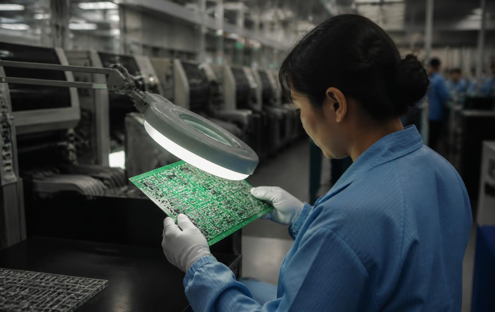
A complete handoff package prevents most quoting delays: Gerbers, an IPC-compliant netlist, a fully specified BOM with manufacturer part numbers, pick-and-place files, assembly drawings, stackup requirements and the test specification. Missing any of these turns a two-day quote into a two-week conversation, and vague BOM lines invite substitutions you did not approve.
Agree in writing how substitutions are handled, who owns stencils and fixtures, what the acceptance criteria are, and how excess and obsolete inventory is treated. Those four clauses cause most of the friction between founders and assemblers.
- Send Gerbers, netlist, BOM with MPNs, centroid, assembly drawing and test spec together.
- Mark do-not-substitute parts explicitly.
- Define acceptance criteria and IPC class before the first build.
- Clarify ownership of stencils, fixtures and programming tools.
- Agree lead-time buffers for long-lead components.
- Require yield and defect Pareto reporting for every build.
Frequently asked questions
What is electronic product design?
Electronic product design is the engineering of a product's electronics from architecture and schematic capture through PCB layout, firmware bring-up, validation builds, regulatory certification and production release.
What is the difference between EVT, DVT and PVT?
EVT proves the design functions, DVT proves it is reliable and compliant across environments and units, and PVT proves the factory can build it repeatably on production tooling.
How much does electronic product design cost?
A mid-complexity connected device typically costs $110,000 to $300,000 in engineering across architecture through PVT, plus $50,000 to $180,000 in builds, tooling and certification.
How long does it take to design an electronic product?
Nine to fourteen months from architecture to mass production, assuming no major respins and components with available lead times.
What the PCB assembly process expects from your design?
A contract manufacturer does not read intent, it reads files. The PCB assembly process runs stencil print, pick and place, reflow, inspection and test, and each stage has tolerances your design either respects or fights.
Send a complete package: Gerbers or ODB++, centroid file, a bill of materials with manufacturer part numbers and approved alternates, panel drawing with fiducials and tooling rails, and a test plan that states what a pass looks like. Missing alternates are the single most common cause of a stalled build.
Work with LA NPDT: if you are moving from here to execution, start with our product development consulting or talk to us about end-to-end product development .
Filed under:EducationInspiration
Services related to this guide
- Product design servicesIndustrial design and CAD taken all the way to manufacturable files.
- Rapid prototypingWorking prototypes in days, from 3D printing to vacuum casting.
- Electronic design servicesSchematic, PCB layout, firmware and bring-up, through to production handoff.
- Product development examplesReal projects we designed, prototyped and shipped.