Tech Talk E17: Heat Shield to Protect Spaceships, Material as Hard as Diamond, Screen Printing Electronics
A heat shield that better protects spaceships, rockets, and jet aircraft. Cross linked carbon nanotubes that they believe to be extremely strong.
November 21, 20198 min read

Written by Konstantin Dolgan, Ph.D., NPDP
Founder & CEO, Product Development Engineer
Published November 21, 2019Updated September 2, 2026
Tech Talk Episode 17: Heat Shield to Protect Spaceships, Material as Hard as Diamond, Screen Printing Electronics
We’re warming things up today on LA NPDT Tech Talk, where we bring you the latest developments in science and technology and keep you tuned in the newest gadgets and product innovations across the globe.
Bring on the Heat
A team of researchers from Florida State University is developing a design for a heat shield that better protects spaceships, rockets, and jet aircraft. As flight systems become faster, they need better heat shields to protect them.
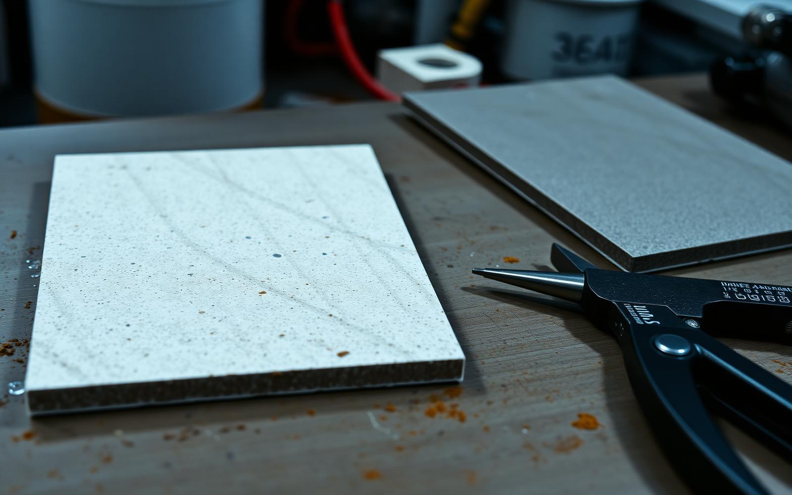
Researchers used sheets of carbon nanotubes in the shape of a cylinder to build the heat shield. The material, known as buckypaper, was soaked in a resin of phenol to create lightweight, flexible material that is durable enough to potentially protect the body of a rocket or jet.
This thin shield protects and supports the body of the rocket. Early tests show that the buckypaper shields are better at dispersing the heat than today’s control shields. While this is good news for the space program, additional research and testing is being done to confirm these findings.
A Material as Hard as Diamonds?
Brown School of Engineering researchers and their colleagues are testing theoretical structures of cross linked carbon nanotubes that they believe to be extremely strong. They 3D printed these polymer blocks and tested them to see this extraordinary strength. The result?
They deflected bullets and withstood crushing forces up to 10 times better than a solid block of the material. The lab tests showed how the porous polymer lattice let the blocks collapse in without cracking, essentially “catching” the bullet.
The material, almost as hard as diamonds, could lead to new safety features for law enforcement, the military, and other EMS services.
Screen Printing Electronics
Researchers have shown that it is possible to print large scale integrated circuits in a printing press. The researchers, from Linkoping University and RISE, Campus Norrkoping, have shown that we can print circuits with more than 100 organic electrochemical transistors.
By using a precise screen printer and the right material, they have been able to print circuits that can be used to power an electrochromic display or other parts of the world that the internet of things brings to reality.
New Material Developments and Applications
Technology Area | Material / Method | Potential Application |
|---|---|---|
Heat Shield | Buckypaper (carbon nanotubes + phenol resin) | Protect spaceships, rockets, jet aircraft |
Strong Material | Cross-linked carbon nanotubes (3D printed polymer blocks) | Safety features for law enforcement, military, EMS |
Electronics Printing | Screen printing with organic electrochemical transistors | Power electrochromic displays, Internet of Things components |
Why printed electronics manufacturing matters to product teams
Screen-printed integrated circuits are a research headline, but the underlying shift is practical: printed electronics manufacturing turns conductive inks and thin flexible substrates into functional circuits using processes borrowed from graphics printing rather than from silicon fabs.
For a product team, that changes where sensing and interface electronics can live — inside a curved housing, laminated behind a membrane, or printed directly onto packaging that ships by the million.
The trade is performance for form and cost. Printed transistors switch far slower than silicon and carry less current, so they will not run a processor. They are well suited to low-frequency roles: capacitive touch layers, antennas, heaters, electrochromic displays, moisture and strain sensors, and simple logic close to the sensor. In most designs the printed layer feeds a conventional silicon controller on a small rigid board.
Where printed electronics fits today
Application | Typical process | Why printing wins | Watch out for |
|---|---|---|---|
Capacitive touch surfaces | Screen-printed silver on PET | Conforms to curves, thin, cheap at volume | Silver ink cost, trace resistance over long runs |
RFID and NFC antennas | Rotary screen or flexo | Roll-to-roll cost per unit is fractions of a cent | Tuning shifts with substrate and adhesive |
Flexible heaters | Carbon or silver ink on polyimide | Even heat over an odd shape | Hot spots at bends; validate with thermal imaging |
Skin and wearable sensors | Inkjet on TPU | Stretchable, disposable, conformal | Crack propagation after repeated strain cycles |
Smart packaging and labels | Flexo or gravure | Prints inline with existing label runs | Shelf life of the ink and encapsulation |
Design rules that differ from a rigid PCB
- Trace width is set by resistance, not current density. Printed silver is roughly ten to a hundred times more resistive than copper foil, so long runs need wide traces or a copper jumper.
- Layer count stays low. Two conductive layers plus a dielectric crossover is a normal ceiling; route accordingly rather than assuming a four-layer stack.
- Bend radius is a real constraint. Keep conductors out of the tightest fold, and put crossovers and component pads in flat zones.
- Substrate temperature limits the ink. PET tolerates roughly 130 °C, polyimide far more; low-temperature sintering inks exist but cost more and cure slower.
- Assembly attaches with conductive adhesive. Standard reflow will destroy most flexible substrates, so silicon parts are bonded with anisotropic film or low-temperature solder.
Advanced materials news — heat shields, superhard carbon, printed circuits — usually reaches products through this path: a lab proves a property, a process engineer finds a way to deposit it repeatably, and a product team decides whether the new capability removes a part, a step or a failure mode. If it does not do one of those three things, it stays a paper. That filter is worth applying to every material announcement you read.
How to evaluate a new material for your product
- Name the incumbent material and the specific property that is failing you — mass, temperature, stiffness, cost, cycle time.
- Ask for the supplier's data at your operating condition, not at the headline condition, and for the test standard used.
- Confirm a production form factor exists: sheet, pellet, ink, prepreg. Lab-scale grams do not become an injection-molded part.
- Price it as an assembly, not per kilogram. A costlier material that deletes two parts and a fastener often wins.
- Run a small physical trial before design freeze; adhesion, finish and joining behavior rarely match the datasheet.
Choosing materials and processes together is core product design work, and it is where an early prototype pays for itself. If you are weighing a new material or a printed sensor layer for a product in development, our rapid prototyping team can build the test coupon before you commit to tooling.
Frequently asked questions
What materials are being developed for advanced heat shields?
Researchers at Florida State University are developing heat shields using sheets of carbon nanotubes. These nanotubes, known as buckypaper, are soaked in a phenol resin. The resulting material is lightweight, flexible, and durable. Early tests indicate these buckypaper shields disperse heat better than current control shields, offering improved protection for spaceships, rockets, and jet aircraft.
What is the potential of the new extremely strong material being developed?
Brown School of Engineering researchers and colleagues are testing cross-linked carbon nanotube structures. They 3D printed polymer blocks, which deflected bullets and withstood crushing forces 10 times better than solid material blocks. This porous polymer lattice collapses without cracking, effectively 'catching' bullets. The material, almost as hard as diamonds, could enhance safety features for law enforcement, military, and EMS services.
How are integrated circuits being printed?
Researchers from Linkoping University and RISE, Campus Norrkoping, have demonstrated printing large-scale integrated circuits using a printing press. They have printed circuits containing over 100 organic electrochemical transistors. By utilizing a precise screen printer and appropriate materials, these circuits can power electrochromic displays or other Internet of Things components. This method allows for the production of circuits in a printing press.
What benefits do buckypaper heat shields offer?
Buckypaper heat shields are designed to protect spaceships, rockets, and jet aircraft. They are made from carbon nanotubes soaked in phenol resin, creating a lightweight, flexible, and durable material. Early tests show these shields are better at dispersing heat compared to current control shields. This thin shield protects and supports the body of a rocket, allowing for potentially faster flight systems.
Sources and standards
- USPTO — patent basics — Official guidance on provisional and non-provisional filings for new products.
- NIST Manufacturing Extension Partnership — Federal program supporting US small and mid-size manufacturers.
- ISO 9001 quality management — The quality-system standard most contract manufacturers are audited against.
Choosing a printed electronics process
Printed electronics manufacturing spans several processes with very different economics. Screen printing dominates today for volume and robustness; inkjet and aerosol jet win where the pattern changes often or the substrate is awkward. Choosing on volume and pattern stability, rather than novelty, avoids expensive experimentation.
Process comparison
Process | Best volume range | Minimum feature | Tooling | Typical uses |
|---|---|---|---|---|
Screen printing | 1,000+ | ~100 microns | Screens per layer | Heaters, antennas, membrane switches |
Inkjet | 1-5,000 | ~30-50 microns | None (digital) | Prototypes, variable patterns |
Aerosol jet | 1-1,000 | ~10 microns | None (digital) | Fine features, 3D surfaces |
Flexography | 100,000+ | ~50 microns | Plates | Very high volume roll-to-roll |
Gravure | 1,000,000+ | ~20 microns | Engraved cylinders | Mass volume, high consistency |
Hybrid printed plus SMT | 1,000+ | N/A | Screens plus assembly | Printed traces with placed components |
Whatever the process, qualify the substrate and the cure step together. Most printed electronics failures trace to adhesion or to a cure profile the substrate cannot tolerate, not to the conductive ink itself.
Evaluation checklist
- Test adhesion and flex endurance on the exact substrate you will use.
- Confirm the cure temperature is within the substrate's limit.
- Measure sheet resistance across the whole printed area, not one point.
- Environmental-cycle samples for humidity and temperature.
- Define how printed circuits will be terminated or connected.
Key takeaways
- Choose a printing process by volume and pattern stability.
- Substrate adhesion and cure profile cause most failures, not the ink.
- Plan the termination method early; it constrains the layout.
Advanced materials in real products: what survives the transition
Heat shields that outperform ceramics, coatings as hard as diamond and circuits printed directly onto fabric all begin the same way: a paper demonstrating a property under controlled conditions.
What determines whether the property becomes a product is availability at commercial quantity, behaviour after aging, and whether a supplier will guarantee lot-to-lot consistency. Most materials that make headlines never clear those three hurdles, and the ones that do usually take a decade.
For a product team, the practical skill is reading a material claim and finding the omitted conditions. A hardness figure without a test method is decorative. A thermal rating without a duration is meaningless — surviving 1,500 °C for four seconds and for four hours are different materials. A printed conductor's resistance matters far less than how that resistance drifts after five hundred flex cycles and a humidity soak.

Headline claim | Missing condition to request | Why it matters |
|---|---|---|
Withstands extreme heat | Duration, cycle count, atmosphere | Brief peak exposure differs from sustained service |
As hard as diamond | Test method and coating thickness | Thin superhard coatings spall off soft substrates |
Flexible printed circuit on fabric | Flex cycles to failure, wash cycles | Resistance drift, not initial resistance, ends the product |
Self-healing polymer | Healing temperature and time | Many need heat the product will never see |
Bio-based / compostable | Certification and end-of-life facility | Industrial composting is rarely available to consumers |
Screen-printed and flexible electronics: where they work today
Printed electronics are genuinely production-ready for a narrow set of functions: membrane switches, capacitive touch overlays, heaters, antennas, and simple sensor traces. They are not ready to replace a populated circuit board with fine-pitch silicon. The value is not lower cost per circuit — it is the ability to put a conductive layer on a curved, thin or flexible surface where a rigid board cannot go.
Design constraints follow from the substrate. Silver inks are the reliable choice and the expensive one; carbon inks are cheap and far more resistive. Trace geometry must tolerate ink spread, and every crossover needs a printed dielectric layer that adds a process step.
Interconnection to the rigid world — the crimp, the ZIF connector, the anisotropic conductive film bond — is where most printed assemblies fail in the field, so it deserves the majority of your test budget.
- Fix the substrate first; the ink system and the process window follow from it
- Specify silver where resistance matters and carbon only for shunts, shields and low-current sensing
- Budget a printed dielectric layer for every crossover in the layout
- Test the rigid-to-flex interconnect to five times the expected field cycle count
- Run humidity and temperature soaks before finalizing the ink, not after tooling the die
- Ask the printer for their registration tolerance and design the layout inside it
These decisions belong with the electronics architecture rather than with industrial design, which is why we handle them inside electronic design services and validate them against the manufacturing plan during production planning.
Frequently asked questions
How long does a new material take to reach production? Typically five to fifteen years from first publication to a qualified commercial grade with multiple suppliers. Products that depend on a single-source research material carry existential supply risk.
Can I design around a material that is not yet commercially available? Only with a conventional fallback in the same envelope. Otherwise a supplier decision you do not control determines whether your product exists.
Are printed electronics cheaper than a flex PCB? Not usually at low volume. Printed circuits win on form factor and on very high volume with simple geometry; a conventional flex circuit wins on density and on repeatable quality.
What is the most common failure in flexible electronics? The interconnect between the flexible circuit and the rigid board. Design it as a serviceable, testable joint and cycle-test it aggressively — a pattern visible across projects in our portfolio.
Exploring printed or flexible electronics for your product?
Filed under:Tech Talk Podcast
Services related to this guide
- Product design servicesIndustrial design and CAD taken all the way to manufacturable files.
- Rapid prototypingWorking prototypes in days, from 3D printing to vacuum casting.
- Electronic design servicesSchematic, PCB layout, firmware and bring-up, through to production handoff.
- Product development examplesReal projects we designed, prototyped and shipped.