
PCB Design for Manufacturing: Process, Costs and Handoff Checklist
PCB design for manufacturing - stackup and DFM rules, the handoff package your fabricator needs, and what a respin really costs.
April 14, 20166 min read

Written by Konstantin Dolgan, Ph.D., NPDP
Founder & CEO, Product Development Engineer
Published April 14, 2016Updated September 2, 2026
Most hardware delays start on the board. A schematic that never got a second pair of eyes, a connector chosen because it was in stock, a stackup picked by the fabricator instead of the designer - each one costs a respin. PCB design services exist to compress that risk into a paid, reviewable process with defined deliverables. Here is how the work is actually structured, what it costs, and what a designer needs from you before day one.
What do PCB design services include?
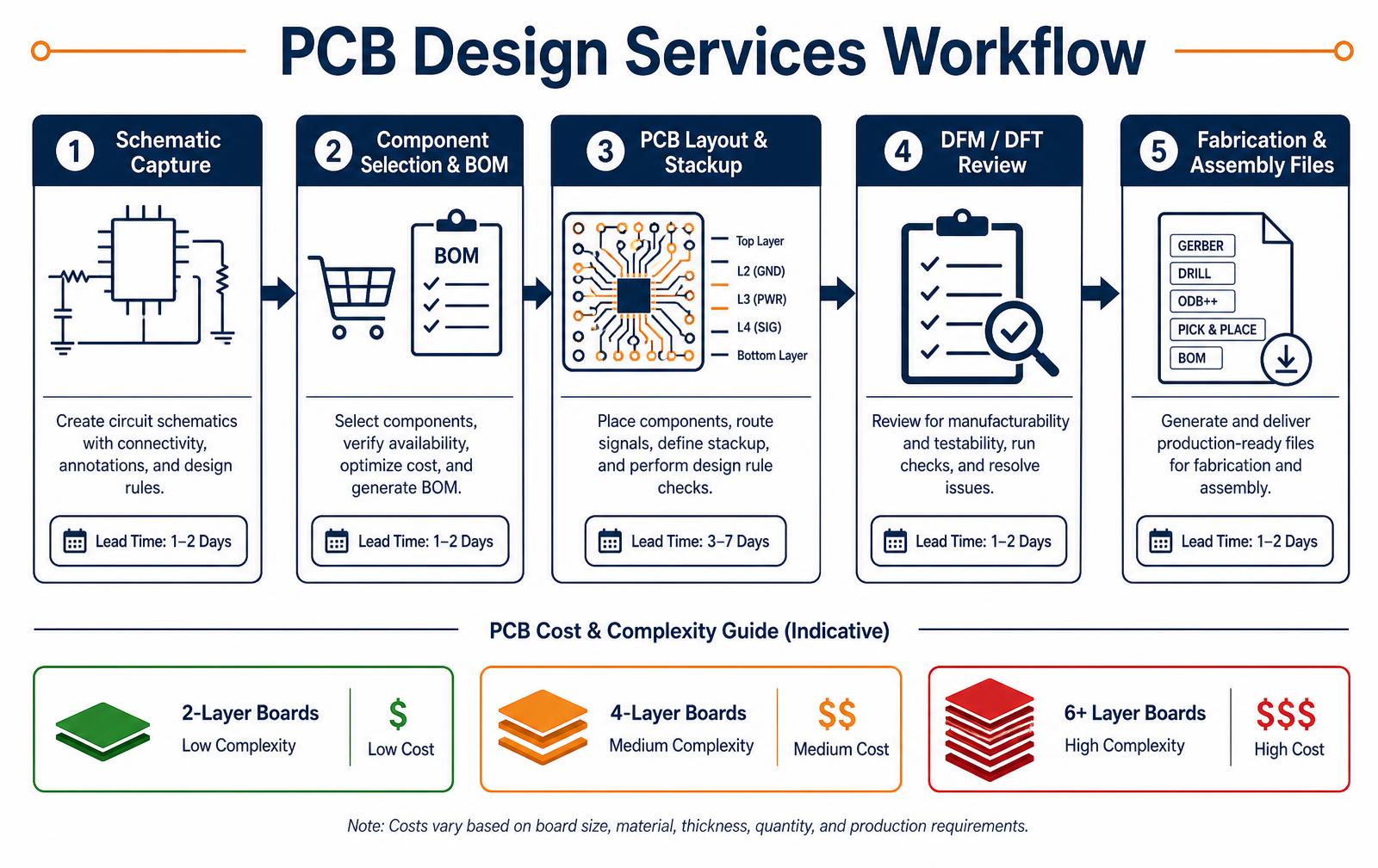
A complete engagement is not just layout. It starts with a requirements pass - supply voltages, interfaces, current budget, enclosure envelope, certification target - and ends with a released file package a fabricator can build without asking questions. Layout is the visible middle. The value is in the decisions on either side of it.
- Architecture and schematic capture - block diagram, power tree, net naming and design rules agreed before a single trace is drawn.
- Component selection and BOM - parts chosen for lifecycle and availability, with second sources named for anything single-sourced.
- Stackup and layout - layer count, impedance control, return paths, thermal relief and placement for assembly.
- Signal and power integrity review - length matching, decoupling strategy, and simulation when interfaces exceed a few hundred megahertz.
- DFM and DFT review - clearances, panelization, test points and programming access checked against the chosen assembly house.
- Release package - Gerber or ODB++, drill files, pick and place, assembly drawings, netlist and a fully sourced BOM.
How much do PCB design services cost?
Pricing tracks complexity far more than board size. A two-layer sensor board with a microcontroller and a regulator is a week of work. A six-layer board carrying DDR, a wireless module and a switching supply is a month, and the review effort scales with it. Rates in the United States generally run $95 to $180 per hour, and most firms quote fixed fee once the schematic is agreed.
Board class | Layers | Typical design effort | Design fee | Prototype fab and assembly |
|---|---|---|---|---|
Simple sensor or breakout | 2 | 20-40 hours | $2,500-$6,000 | $300-$900 for 5 boards |
Microcontroller product board | 4 | 60-120 hours | $7,000-$18,000 | $900-$2,500 for 5 boards |
Wireless or mixed-signal | 4-6 | 120-200 hours | $18,000-$35,000 | $1,500-$4,000 for 5 boards |
High-speed compute or DDR | 8-12 | 200-400 hours | $35,000-$80,000 | $3,000-$9,000 for 5 boards |
How long does PCB design take?
- Week 1 - requirements, power tree, part selection and long-lead purchase decisions.
- Weeks 2-3 - schematic capture and design review with the firmware and mechanical owners in the room.
- Weeks 3-5 - placement, routing, stackup confirmation with the fabricator and DFM iteration.
- Week 5 - file release; fabrication runs 3-10 days standard, 24-72 hours expedited.
- Weeks 6-8 - assembly, bring-up and the errata list that drives revision B.
What to send a PCB designer before day one
- A written functional spec: what the board does, what it connects to, and how it is powered.
- The mechanical envelope - a STEP file of the enclosure with mounting holes and connector positions, not a sketch.
- Current draw per rail and the worst-case thermal environment.
- Certification targets - FCC, CE, UL, IEC 60601 - because they change spacing, filtering and shielding decisions.
- Volume expectations for year one, which decide whether to optimize for unit cost or for speed.
- Any firmware constraints: debug interface, bootloader, programming method used in production.
Avoiding the second respin
Almost every board gets a revision B. The teams that stop there do three things: they hold a formal schematic review with firmware and manufacturing present, they populate test points and programming headers for production rather than for the bench, and they send the layout to the actual assembly house for DFM feedback before release, not after. Related reading: our electronics design services and rapid prototyping.
Design for manufacturing rules that prevent respins
Assembly houses do not redesign your board. They build what the files say and report the yield. Most first-run assembly problems trace back to a handful of layout decisions that cost nothing at design time and thousands to correct after the panel is fabricated.
DFM rule | Why it matters | Typical requirement |
|---|---|---|
Component courtyard spacing | Placement head and rework access | 0.5 mm minimum between courtyards, 1 mm near tall parts |
Board edge clearance | Conveyor rails grip the edge | 3 mm clear of components on two opposing edges |
Fiducials | Machine vision alignment | Three global fiducials plus local fiducials on fine-pitch parts |
Thermal relief on ground pads | Prevents cold solder joints | Spoked connections on through-hole pads tied to planes |
Test point coverage | In-circuit and functional test access | 1 mm pads on every net, single-sided where possible |
Panelization | Handling and depaneling stress | V-score for straight edges, tab-route with mouse bites for profiles |
Polarity and pin-1 markings | Assembly and rework accuracy | Silkscreen indicators visible after assembly |
Paste layer tuning | Solder volume on QFN and BGA | Windowpane large thermal pads to 50-70% aperture |
The handoff package that gets a clean quote
Fabricators and assemblers price uncertainty. An incomplete package returns a padded quote and a list of engineering questions that add a week before anything is built. A complete package returns a firm price and a build slot.
- Gerber X2 or ODB++ output with a fabrication drawing that states stackup, material, finish and impedance targets.
- NC drill files with plated and non-plated holes separated and clearly identified.
- Centroid or pick-and-place file with reference designator, X, Y, rotation and layer for every placed part.
- Bill of materials with manufacturer part numbers, approved alternates and do-not-populate lines called out explicitly.
- Assembly drawing showing orientation, connector keying and any hand-soldered or post-process steps.
- Paste stencil requirements, including any reduced apertures.
- Test requirements: what the assembler must verify before shipping, and what you will verify at bring-up.
Costs that surprise first-time teams
Item | Typical cost | Notes |
|---|---|---|
Stencil | $150-$400 | One per revision; changes with paste layer edits |
Assembly NRE and programming | $300-$1,200 per revision | Charged again after any placement change |
Impedance-controlled stackup | 10-25% fab premium | Required for USB, Ethernet, RF and DDR |
Expedited fab (24-72 hours) | 2-4x standard price | Budget one expedite per project, not three |
Functional test fixture | $3,000-$15,000 | Worth it above roughly 500 units per year |
Respin (fab plus assembly plus time) | $4,000-$15,000 plus 3-4 weeks | The cost every DFM rule above is trying to avoid |
Key takeaways
- Most respins come from files and DFM detail, not from circuit design errors.
- A complete handoff package buys a firm price and a faster build slot.
- Design test access in from the start; retrofitting test points requires a new revision.
- Budget two board spins on any non-trivial design and treat the third as a process problem.
Stackup and impedance decisions made before layout
The single decision with the biggest effect on both PCB cost and signal integrity is the layer stackup, and it has to be made before routing begins. Adding layers late means re-routing; discovering an impedance requirement late means the same. Agree the stackup with your fabricator, in writing, at the start of layout.
Stackup choices and their consequences
Layers | Typical use | Relative bare-board cost | Constraints |
|---|---|---|---|
2 | Simple analog, low-speed digital | 1.0x | No dedicated ground plane, poor EMC |
4 | Most embedded products | 1.5-2x | Good ground plane, limited routing density |
6 | Dense digital, one radio | 2.5-3.5x | Room for controlled impedance |
8+ | High-speed interfaces, BGA fanout | 4x and up | Requires impedance control and careful cost review |
HDI / microvias | Fine-pitch BGAs, compact devices | 2-4x on top of layer count | Fewer fabricators, longer lead time |
Controlled impedance adds test coupons and a fabrication note but rarely much money on a modest board — far less than a respin caused by an unroutable high-speed pair. Specify it whenever you have USB, Ethernet, DDR or an antenna feed.
Pre-layout decisions to lock down
- Layer count and stackup, confirmed with the chosen fabricator.
- Impedance targets for every high-speed net class.
- Minimum trace, space and drill sizes matched to standard fab capability.
- Board outline, mounting holes and connector positions from the mechanical model.
- Test point strategy and any in-circuit test requirements.
Key takeaways
- Stackup is a pre-layout decision; changing it later means re-routing.
- Controlled impedance is cheap insurance on any high-speed or RF board.
- Match design rules to standard fabricator capability to avoid premium pricing.
PCB design for manufacturing: the review that saves a spin
Most board respins are avoidable and traceable to a review that never happened.
Before releasing, walk the layout with the fabricator and the assembler in the room: minimum trace and space against their standard process, annular ring and drill sizes against their cheapest class, panelisation and depanel method, component keep-outs for the test fixture, and a stackup the fab actually stocks.
Designing to a class the shop rarely runs adds cost and yield loss for no functional gain.
- Match the fab class. Ask what their standard process handles before pushing trace geometry.
- Stackup from stock. Custom laminate combinations add weeks of lead time.
- Plan the panel. Rails, fiducials and depanel routing belong in the first layout, not the last.
- Design for test. Test points on a grid save fixture cost and debug time.
- Second-source critical parts. One sole-sourced regulator can stall an entire build.
Need a PCB designed right the first time?
Work with LA NPDT: if you are moving from here to execution, start with our our product development process or talk to us about end-to-end product development.
Frequently asked questions
What are PCB design services?
PCB design services cover schematic capture, component selection, board layout, signal and power integrity review, DFM checks and release of manufacturing files, so an electronic product can be fabricated and assembled without further engineering.
How much does PCB layout cost?
A simple two-layer board typically costs $2,500 to $6,000 to design. Four-layer product boards run $7,000 to $18,000, and high-speed multilayer designs reach $35,000 to $80,000 at United States rates of roughly $95 to $180 per hour.
How long does it take to design a PCB?
Most product boards take four to six weeks from requirements to released files, plus one to two weeks for fabrication and assembly of the first prototypes.
Should I use a freelancer or a design firm?
A freelancer is efficient for a well-specified single board. A firm is worth the premium when the board is one part of a product that also needs mechanical design, firmware, compliance testing and a manufacturing handoff, because the interfaces between those disciplines are where schedules break.
Filed under:Media
Services related to this guide
- Product design servicesIndustrial design and CAD taken all the way to manufacturable files.
- Rapid prototypingWorking prototypes in days, from 3D printing to vacuum casting.
- Electronic design servicesSchematic, PCB layout, firmware and bring-up, through to production handoff.
- Product development examplesReal projects we designed, prototyped and shipped.