Electronic product prototyping: from dev board to custom PCB
The three hardware stages every connected product goes through, what each one proves, and when it is time to stop breadboarding and lay out a real board.
August 29, 20261 min read

Written by Konstantin Dolgan, Ph.D., NPDP
Founder & CEO, Product Development Engineer
Published August 29, 2026
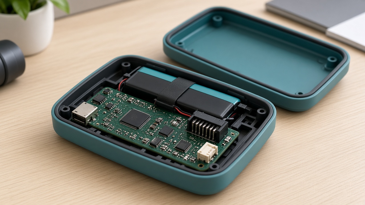
Electronic prototyping goes through three stages: a dev board proof, a custom PCB, and a design verification build in the real enclosure. Skipping the middle stage is the single most common reason a connected product misses its launch date, because a working breadboard tells you nothing about antenna performance, power draw or thermal behavior inside a sealed housing.
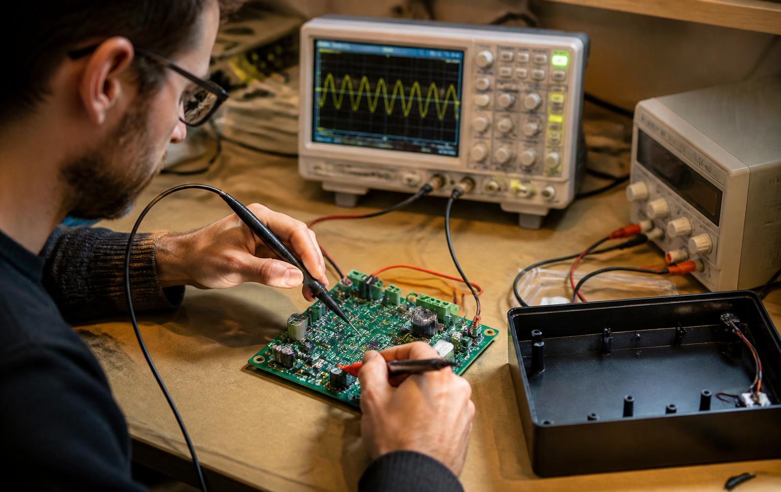
What are the stages of electronics prototyping?
Stage | What it proves | Time | Cost |
|---|---|---|---|
Dev board proof | The sensors, radio and logic can do the job | 2 - 5 weeks | $5,000 - $20,000 |
Custom PCB revision A | Real layout, real power budget, real size | 6 - 10 weeks | $15,000 - $60,000 |
Revision B plus DVT build | It works inside the enclosure, at temperature, repeatably | 8 - 14 weeks | $25,000 - $90,000 |
Pre-certification scan | Radiated emissions before you book a lab | 1 - 2 weeks | $1,500 - $5,000 |
When should you stop using a dev board?
- The mechanism is proven and the remaining questions are about size, power or cost.
- You need to hand a unit to someone outside the team.
- Battery life matters and you cannot measure it honestly on a dev kit.
- You have wireless and need to know how the antenna behaves next to a battery and a plastic wall.
- You want a manufacturing quote, which requires a real bill of materials.
What usually breaks on revision A
Expect two board revisions. The first one nearly always reveals a power sequencing issue, an antenna keepout violation, a footprint mistake on one part, or a regulator that gets hotter than the datasheet suggested. That is normal engineering, not failure. Budget for it up front so it does not read as a surprise to your investors.
Firmware and certification timing
Firmware should start on the dev board and continue on revision A, not begin after hardware is final. FCC and CE testing needs stable hardware and firmware in a final housing, and lab slots are booked weeks out. Run a pre-scan at a local lab before the formal test; failing the formal test costs both the fee and the calendar.
Where LA NPDT fits
We do the schematic, layout, firmware and enclosure together, so the board and housing are designed against each other rather than in sequence. See electronic design services, the SmartVue PCB enclosure case study, or the path from prototype to production.
Proof from our own work: see the full electronics path on the QMS2GO voice recorder, from board bring-up to a molded, shippable product.
Have a board to design?
Send us the requirements and we will scope the electronics path.
Services related to this guide
- Electronic design servicesSchematic, PCB layout, firmware and bring-up, through to production handoff.
- Rapid prototypingWorking prototypes in days, from 3D printing to vacuum casting.
- Product design servicesIndustrial design and CAD taken all the way to manufacturable files.
- Product development examplesReal projects we designed, prototyped and shipped.