Enclosure design for electronics: a practical checklist from board envelope to sealed housing
Enclosure design for electronics is co-designing the board, battery, connectors, and housing as one system: shared envelope, seals, thermals, RF keepouts, and assembly access before tooling.
September 30, 20264 min read

Written by Konstantin Dolgan, Ph.D., NPDP
Founder & CEO, Product Development Engineer
Published September 30, 2026
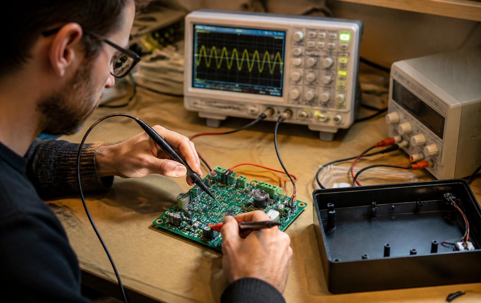
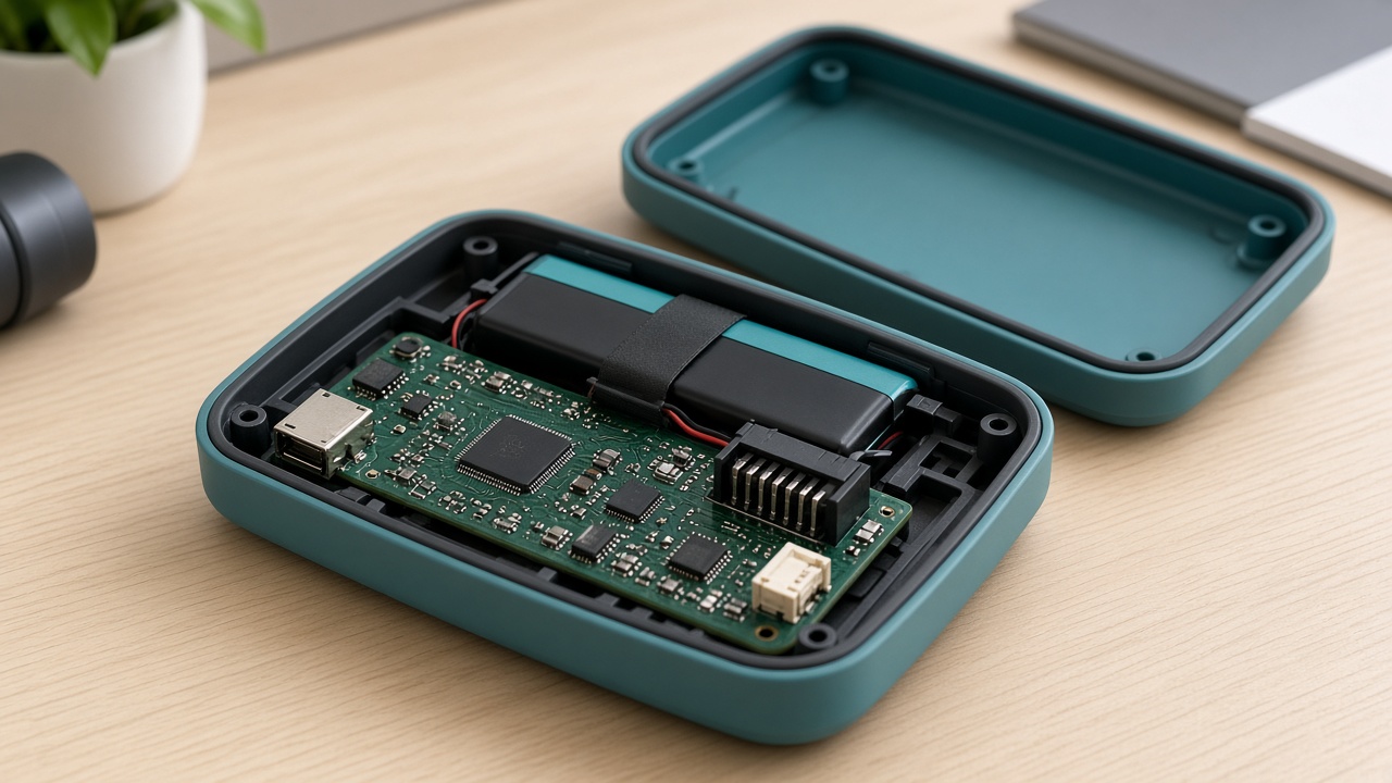
Enclosure design for electronics means making the board, battery, connectors, controls, and housing work as one buildable system. The useful starting point is a shared envelope, not a pretty shell drawn after the PCB freezes. That shared model lets the team resolve fit, sealing, cooling, antenna space, and assembly access while changes are still practical.
Key takeaways
- Freeze the board envelope first. Lock the outline, height, keepouts, and connector faces before polishing the industrial design.
- Make interfaces explicit. Mounting, gasket paths, vents, and antenna keepouts are requirements, not late CAD notes.
- Design for hands and tools. Screws a line worker can reach are better than glamorous snaps that trap a PCB.
- Build around a real board revision. A looks-like shell alone will not reveal thermal, RF, connector, or sealing failures.
- Keep ownership clear. If you want one team working across board and housing, talk to an engineer before either side freezes.
What enclosure design for electronics actually decides
The enclosure decides more than fit. It helps define the environment claim, assembly effort, service access, RF path, grounding strategy, touch surfaces, and the safety boundary around power and moving parts. Good electronic design and product design therefore move together.
A freeze-then-box workflow pushes every conflict into the housing. Connector cutouts become awkward, batteries occupy leftover space, antennas sit beside metal or noisy electronics, and screws become hard to reach. Co-design exposes those conflicts while board outlines, component placement, and housing geometry can still trade space deliberately.
Start with the board envelope, not the pretty shell
Create one controlled STEP envelope that both electrical and mechanical teams use. It should include the product outer dimensions, PCB outline and thickness, component height zones, keepouts, connector and user-interface faces, battery volume, mounting datums, cable exits, and any surfaces that must remain clear.
The envelope is a coordination model, not final industrial design. Update it when a connector, battery, display, heat source, or antenna moves. For a broader board-to-build sequence, see the electronic product prototyping guide.
Mechanical enclosure checklist
Check | What to decide before tooling | Why it matters |
|---|---|---|
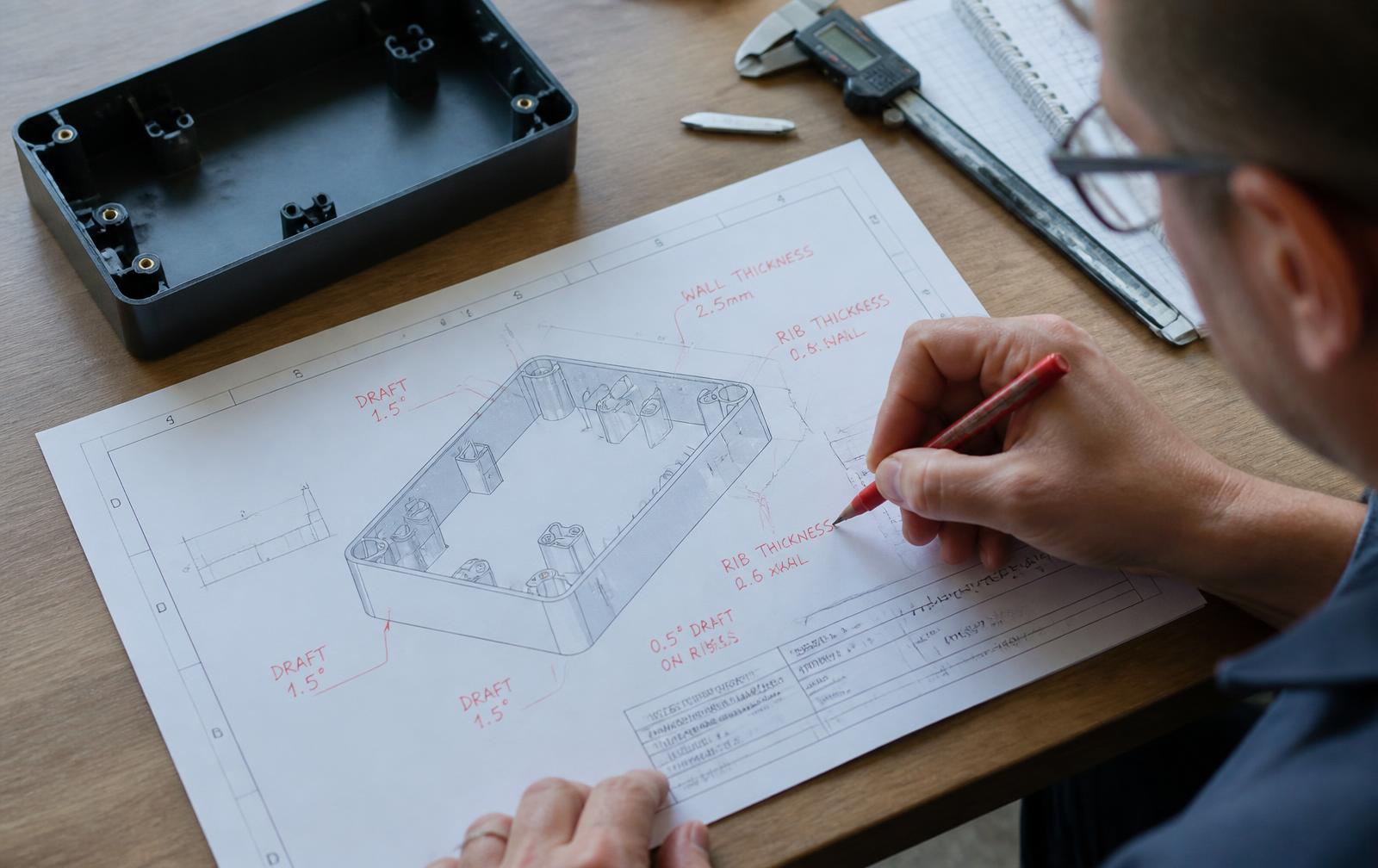
Uniform wall thickness | Set a process-appropriate wall strategy and manage necessary transitions. | Reduces avoidable sink, warp, and uneven cooling risk. |
Draft | Identify pull direction and add draft to walls, ribs, bosses, and texture-sensitive faces. | Allows molded parts to release without damaging the intended finish. |
Boss height and core-out | Support bosses with ribs where needed and avoid isolated thick masses. | Keeps mounting features stable without concentrating material. |
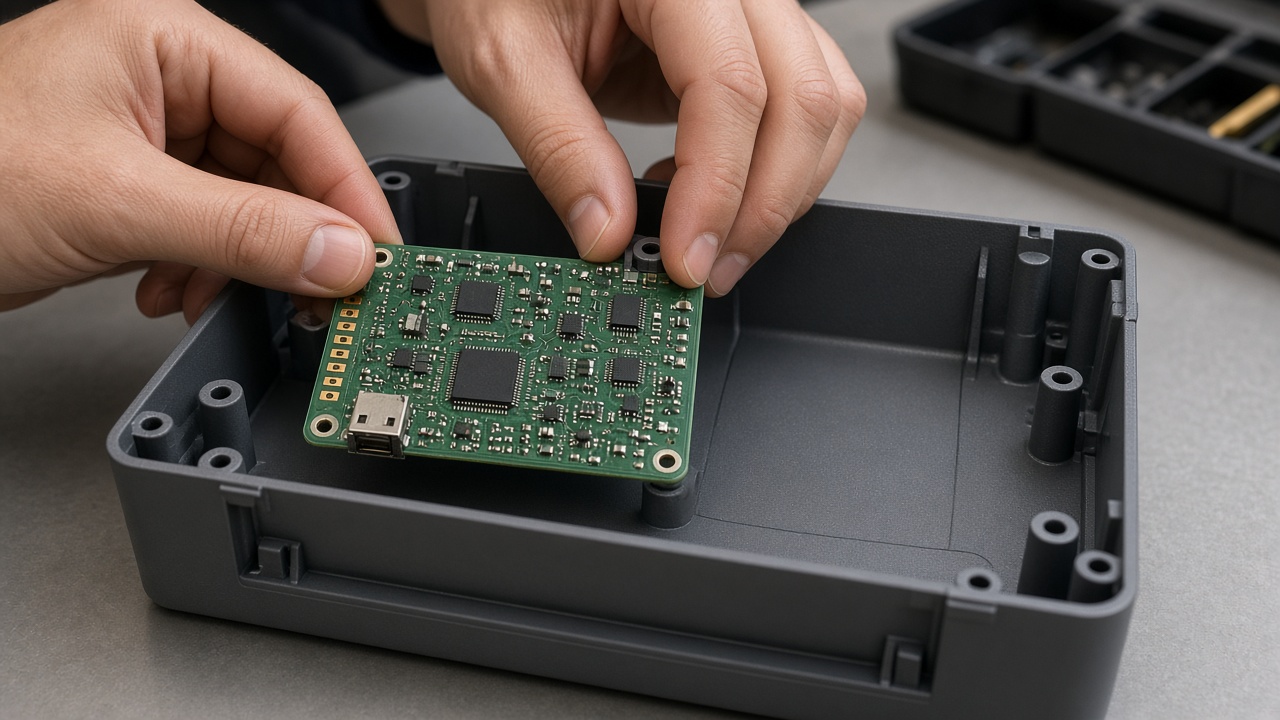
Screw access and assembly order | Show driver approach, fastener list, torque intent, and the order parts are installed. | Prevents blocked fasteners and fragile late-stage assembly moves. |
Gasket gland | Define the continuous seal path, corners, joints, compression intent, and how the halves locate. | A gasket only works when its geometry and compression are controlled. |
Cable glands and strain relief | Name cable exits, bend space, retention, sealing, and pull-load path. | Protects conductors and keeps cable loads away from solder joints. |
Service openings | Define access to debug headers, batteries, ports, filters, and replaceable items. | Avoids dismantling the product for routine work and diagnosis. |
Run this table as part of a formal design for manufacturing review before any hard tooling purchase order. The review should follow the intended process and assembly sequence, not a generic checklist applied without context.
Electrical and RF interfaces belong in the housing model
- Antenna keepouts: reserve clear volume around the antenna and keep likely metal, batteries, cables, and noisy electronics out of that zone.
- Grounding and EMI: identify shields, conductive contacts, seams, cable paths, and enclosure features that support the grounding strategy.
- Connector faces: control connector position, shell clearance, flush condition, mating access, and sealing details from shared datums.
- Display and button stacks: model lens, adhesive, light guides, switches, elastomers, travel, and compression as one tolerance chain.
- Wireless validation: test the radio in a production-representative housing because wall material, coatings, batteries, and nearby hardware can change performance.
Thermal, IP, and Emi Checks Without Guessing
Design toward the environment you plan to claim. The IEC overview for IEC 60529 defines the IP classification system for enclosure protection. If the product will carry an IP claim, translate that claim into a continuous seal path, controlled openings, cable interfaces, assembly controls, and a test plan.
Thermal and EMI work also needs the intended shell. Measure the hottest components and touch surfaces on a works-like unit, with realistic power states and airflow. Pre-scan electronics in the intended enclosure with representative cables, seams, shields, and grounding features. The enclosure thermal design white paper is a useful engineering reference, but the product-specific answer still comes from measurement.
A prototype sequence that retires the right risks
Build | What it should answer | What it does not prove |
|---|---|---|
Looks-like | Overall size, form, controls, grip, access, and visual direction. | Heat, radio performance, sealing, or repeatable assembly. |
Works-like | Board fit, connector alignment, mounting, cables, controls, firmware use, thermal behavior, and wireless behavior. | Final environmental performance or production repeatability. |
Sealed environmental | Gasket path, cable exits, service openings, closure sequence, and the planned dust or water test. | Tooling capability or stable production variation. |
Production-intent | Manufacturing process, material, fasteners, finishes, assembly sequence, inspection points, and critical fits. | Ongoing process control without first-article and production inspection. |
Hybrid prototyping can combine printed, machined, fabricated, and production-like parts when one process cannot answer every question. The goal is not a perfect model in one pass. It is a deliberate sequence from appearance to function, then environment and production intent. See the wider prototype-to-production steps for the surrounding program gates.
Founder checklist before enclosure tooling
- Shared STEP envelope: PCB, battery, connectors, and keepouts are current and controlled.
- Mounting plan: datums, screw list, driver access, and assembly order are defined.
- Environment interfaces: gasket path and cable exits are named for the target environment.
- RF and EMI: antenna and EMI features are specified, or the project explicitly records that they are not required.
- Thermal plan: the hottest components and intended touch temperatures have a measurement plan.
- Service access: debug, charging, battery, and maintenance access are defined.
- Works-like build: the housing build is scheduled against a real or revision-close board.
- DFM gate: the team will complete a DFM review before any hard tooling purchase order.
- First article: inspection covers critical fits, connector positions, fastener access, and seal compression.
Where LA NPDT fits
LA NPDT can work across the board envelope, industrial design, mechanical package, prototype builds, and manufacturing review so the electrical and mechanical decisions stay synchronized. The public SmartVue PCB enclosure design portfolio shows the kind of board-and-housing coordination this article describes.
If the project is still being scoped, you can apply to partner with us. If the board already exists, bring the current STEP file, connector map, battery choice, and intended environment to the first discussion.
Have a board and need a housing plan?
Talk with an engineer about co-designing the board and enclosure before either freezes.
Frequently asked questions
What is enclosure design for electronics?
It is the mechanical and systems work that packages a PCB, power source, and connectors into a housing that meets fit, environment, assembly, and user-interface needs. It includes envelopes, seals, thermals, and RF keepouts, not only outer styling.
When should PCB and housing design start together?
Start as soon as the board outline, connectors, and battery volume are known well enough to draw a shared envelope. Waiting until schematic freeze forces expensive carve-outs and leaves less room to resolve mechanical and electrical conflicts.
How is electronics packaging design different from buying an off-the-shelf project box?
An off-the-shelf box can work for low-volume instruments with generous size and simple interfaces. Custom packaging becomes useful when the product needs a specific protection claim, appearance, antenna performance, connector arrangement, or assembly approach at volume.
Do I need an IP-rated enclosure for a consumer desk product?
Only if you claim dust or water protection. Many consumer products need splash resistance and strain relief more than a formal IP rating. If you market an IP rating, design and test the enclosure to IEC 60529.
What prototype proves enclosure design for electronics?
Use a works-like unit with the real or revision-close PCB inside a production-representative housing. Looks-like shells prove size and styling, but they do not prove heat, RF, connector alignment, assembly access, or seal behavior.
Tagged:Electronics
Services related to this guide
- Electronic design servicesSchematic, PCB layout, firmware and bring-up, through to production handoff.
- Rapid prototypingWorking prototypes in days, from 3D printing to vacuum casting.
- Product design servicesIndustrial design and CAD taken all the way to manufacturable files.
- Product development examplesReal projects we designed, prototyped and shipped.