Electronics Design: From Requirements to a Manufacturable PCB
Electronics design moves a product from requirements to a manufacturable PCB. Here is the flow: architecture, schematic, layout, DFM review, bring-up and compliance.
October 14, 20165 min read

Written by Konstantin Dolgan, Ph.D., NPDP
Founder & CEO, Product Development Engineer
Published October 14, 2016Updated September 3, 2026
Electronics design turns a product requirement into a manufacturable circuit board: architecture, schematic, PCB layout, firmware bring-up, EMC compliance and a released manufacturing package. Most schedule slips in hardware are not caused by the circuit being hard. They are caused by requirements that were never written down, and by compliance testing scheduled after the enclosure was tooled.
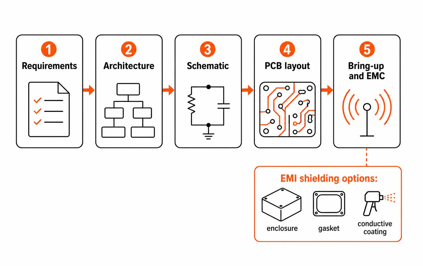
The five phases and what each one produces
Phase | Deliverable | Typical duration | Gate to pass |
|---|---|---|---|
Requirements | Electrical spec: power budget, interfaces, environment, certifications | 1-2 weeks | Every number has a source, not a guess |
Architecture | Block diagram, part selection, risk list | 1-3 weeks | Long-lead and sole-source parts identified |
Schematic | Reviewed schematic and BOM | 2-4 weeks | Peer review signed off, pin-by-pin |
PCB layout | Stackup, layout, Gerbers, assembly drawings | 2-5 weeks | DFM/DFT review with the assembler |
Bring-up and EMC | Test report, errata, released package | 3-8 weeks | Pre-compliance passed before enclosure tooling |
Write the electrical requirements first
- Power. Source, voltage range, peak and average current, battery life target and charge profile.
- Interfaces. Every connector and protocol, including the debug and programming interface you will need in production.
- Environment. Temperature range, humidity, ingress rating, shock and vibration.
- Compliance. Target markets and the standards that follow: FCC Part 15 or CISPR 32, CE, UL, IEC 60601 for medical, radio module certifications.
- Volume and cost. Annual volume and BOM cost target — these decide microcontroller class, layer count and whether you buy a pre-certified radio module.
- Lifecycle. How long the product must ship, which sets part availability and second-source requirements.
PCB layout decisions that determine whether it works
- Stackup before routing. Choose layer count and dielectric with the fab house, then set impedance targets for every controlled-impedance net.
- Continuous reference planes. A split under a high-speed trace forces return current around the gap and turns a signal into an antenna.
- Decoupling placement. Small capacitors close to the pin with short vias to plane; the loop area matters more than the value.
- Partition by noise. Keep switching regulators, RF and sensitive analog in separate regions with deliberate single-point connections.
- Thermal path. Copper pours, thermal vias and component spacing designed against the worst-case power dissipation, not the typical case.
- Design for test. Test points, fiducials, panelization and programming headers agreed with the assembler before Gerbers are released.
emc and Emi Shielding: Plan it, Do not Patch It
Emissions failures are found late and fixed expensively. Book a pre-compliance scan on the first working prototype, while the layout can still change. When suppression at the source is not enough, shielding is the next lever — and each option has a different cost and tooling impact.
Approach | Where it applies | Trade-off |
|---|---|---|
Board-level shield can | A single noisy or sensitive subcircuit | Cheap and local; blocks rework and adds height |
Metal enclosure | Whole-product shielding | Very effective; weight, cost and grounding complexity |
Conductive coating on plastic | Plastic housings that need attenuation | Keeps the plastic enclosure; adds a coating process step |
Gaskets and finger stock | Seams, lids and access panels | Restores shielding at joints; needs compression control |
Filtering and ferrites | Cable-borne emissions | Low cost; only fixes conducted paths |
Graphene-based conductive coatings — the technology behind Grapheno, the startup spun out of our team and covered in the archived post below — sit in that fourth row: attenuation applied to a plastic housing without switching to a metal enclosure.
What causes a second board spin
- Footprints taken from an unverified library instead of the part datasheet.
- No programming or debug access designed in, discovered at assembly.
- Power sequencing missed between rails, leaving a device latched off.
- Connector orientation or keep-out clashing with the mechanical enclosure.
- A part that is obsolete or on 40-week lead time by the time you order.
- Pre-compliance skipped, so a radiated emissions failure arrives after tooling.
Budget for two spins on any non-trivial board and treat the third as a warning sign. Electrical and mechanical work must run together: see electronic design services and end-to-end development for how we pair them, or read the DFM guide.
Planning bring-up before the boards arrive
Bring-up is where schematic optimism meets reality, and the teams that get through it in days rather than weeks wrote the plan before the boards shipped. Power up in stages, instrument each rail, and never apply full power to an unknown board.
Bring-up step | What to verify | Instrument | Typical time |
|---|---|---|---|
Visual and continuity check | Shorts across rails, part orientation, pin 1 | Multimeter, microscope | 1-2 hours |
Current-limited power-on | Inrush and quiescent current against the estimate | Bench supply with limit | 1 hour |
Rail sequencing and ripple | Voltage accuracy, sequence order, noise | Oscilloscope | 2-4 hours |
Clock and reset | Oscillator start-up, reset release timing | Oscilloscope | 1-2 hours |
Debug interface and firmware load | SWD or JTAG connection, first blink | Debugger | 2-6 hours |
Peripheral bring-up | Each bus, sensor and interface individually | Logic analyzer | 1-3 days |
Thermal and load soak | Temperature rise at full duty cycle | Thermal camera | 4-8 hours |
Pre-compliance EMC scan | Radiated emissions margin against limits | Near-field probe, spectrum analyzer | 1 day |

Design for test from the first schematic
- Bring every rail, clock and critical net to a labelled test point placed on one side of the board.
- Add series resistors, jumpers or zero-ohm links to isolate subsystems during debug.
- Include a debug header with programming, reset and a serial console, even on production boards.
- Provide an on-board way to measure current per rail, such as a sense resistor with dedicated pads.
- Add status LEDs on power rails and the main state machine; they answer the first question without instruments.
- Keep a place for a scope ground spring near high-speed signals - long ground leads report noise that is not there.
Component selection risks worth pricing early
Risk | Warning sign | Mitigation |
|---|---|---|
Long lead time | Distributor lead time above 20 weeks | Design in a footprint-compatible alternate at schematic stage |
Single-source part | One manufacturer, no direct equivalent | Abstract the function behind a common interface |
End of life | Not-recommended-for-new-design status | Check lifecycle status on every active part before layout |
Minimum order quantity | MOQ exceeds annual usage | Choose the mainstream part rather than the optimal one |
Counterfeit exposure | Broker pricing far below distributor | Buy only through authorized channels for programmable and RF parts |
Key takeaways
- Write the bring-up plan while the boards are in fabrication, not when they land on the bench.
- Test points, isolation links and a debug header cost cents and save weeks.
- Component lifecycle and lead time belong in the schematic review, not the purchasing stage.
- A pre-compliance scan on the first working unit is the cheapest EMC insurance available.
Certification: what to plan for and what it costs
Compliance is a schedule item with a price, not a formality at the end. The certification set depends on what the product does and where it sells, and each item has both a lab cost and a queue. Book slots before the design freezes; accredited labs commonly run three to six weeks out, and a failed scan means paying for a board spin plus a retest slot.
Test / certification | Applies to | Typical lab cost | Typical duration |
|---|---|---|---|
EMC pre-compliance scan | Any electronic product | $1,500-$5,000 | 1-2 days |
FCC Part 15B (unintentional radiator) | Digital electronics sold in the US | $5,000-$12,000 | 1-2 weeks |
FCC Part 15C / RED (intentional radiator) | Products with a radio, unless a certified module is used | $15,000-$40,000 | 4-8 weeks |
Safety (IEC/UL 62368-1 or 61010) | Mains-powered or high-energy products | $10,000-$35,000 | 6-12 weeks |
Battery transport (UN 38.3) | Any lithium cell or pack shipped | $3,000-$10,000 | 3-6 weeks |
Using a pre-certified radio module removes the most expensive and least predictable line from that table, at a unit-price premium that is easy to justify below roughly 50,000 units a year. Reference designs matter here: follow the module vendor's keep-out, ground and antenna layout exactly, because deviations are what turn a modular grant into a full intentional-radiator test.
Hardware and firmware co-development
Most schedule loss in electronics programs happens at the boundary between the board and the code, when firmware waits for hardware that is waiting for a decision nobody owns. The teams that ship on time overlap the two deliberately.
- Freeze the register-level interface early. Pin maps, bus addresses, interrupt lines and power sequencing belong in a document both disciplines sign before layout.
- Use an evaluation-board stack so firmware development starts eight to twelve weeks before the custom board arrives.
- Design a bootloader and field update path in from the start. Retrofitting update capability after production is the most expensive routine mistake in connected hardware.
- Keep a hardware abstraction layer so a part substitution driven by a lead-time problem touches drivers, not the application.
- Version the firmware against the board revision and refuse to boot on mismatched pairs; mixed-revision debugging burns days.
Plan bring-up as a staged sequence: continuity and shorts, current-limited power-on rail by rail, clocks, then peripherals in dependency order. A board with labelled test points and isolation links typically completes bring-up in two to four days; one without them regularly takes three weeks. See also our end-to-end development services.
From the archive: Grapheno in the final of the BioChallenge competition
Need a board designed and released?
We take electronics from requirements through schematic, layout, bring-up, pre-compliance and a released manufacturing package.
Work with LA NPDT: if you are moving from here to execution, start with our product development consulting or talk to us about end-to-end product development.
Frequently asked questions
What does electronics design include?
It covers electrical requirements, system architecture and part selection, schematic capture, PCB layout and stackup, firmware bring-up, EMC and safety compliance, and the released manufacturing package: Gerbers, BOM, assembly drawings and test procedures.
How long does an electronics design project take?
A straightforward sensor or controller board typically takes 10-16 weeks from requirements to a validated prototype. Wireless, medical or high-speed designs run 20-40 weeks because compliance testing, certification and additional board spins sit on the critical path.
How much does it cost to design a PCB?
A simple two- to four-layer board with a microcontroller commonly runs $15,000-$40,000 in engineering, plus prototype fabrication and assembly. Complex multi-layer designs with wireless, power electronics or medical documentation range from $60,000 to well over $200,000.
When should EMC testing happen?
Run pre-compliance scans on the first working prototype, before the enclosure is tooled. Formal testing at an accredited lab comes once the design is frozen. Finding an emissions problem after tooling usually means paying for both a board spin and a tool change.
Should I use a pre-certified wireless module?
Under roughly 50,000 units per year, almost always yes. A pre-certified module costs more per unit but removes intentional-radiator certification, antenna tuning and most RF layout risk from the schedule. Chip-down designs pay off only at high volume or with unusual form factor constraints.
Filed under:Media
Tagged:Advanced MaterialsBossierConductive CoatingEmi ShieldingGrapheneGraphenohigh-techInnovationLouisianaMaterialsNew OrleansNorth West LouisianaProduct DevelopmentShreveportStartupTechnologyTechnology Commercialization
Services related to this guide
- Product design servicesIndustrial design and CAD taken all the way to manufacturable files.
- Rapid prototypingWorking prototypes in days, from 3D printing to vacuum casting.
- Electronic design servicesSchematic, PCB layout, firmware and bring-up, through to production handoff.
- Product development examplesReal projects we designed, prototyped and shipped.